SIGCOMM'16 Talk Transcription: ClickNP
ClickNP: Highly Flexible and High-Performance Network Processing with Reconfigurable Hardware
Bojie Li, Kun Tan, Layong (Larry) Luo, Yanqing Peng, Renqian Luo, Ningyi Xu, Yongqiang Xiong, Peng Cheng and Enhong Chen.
Proceedings of the 2016 ACM SIGCOMM Conference (SIGCOMM ‘16). [PDF] [Slides]
Transcription with Whisper.
Thanks Professor Nate Foster for the introduction.
Hello everyone.
I’m Bojie Li, a second-year Ph.D. student in a joint research program with USTC and Microsoft Research.
My topic today is ClickNP, a highly flexible and high performance network processing platform with reconfigurable hardware.
I did this work with my collaborators during an internship with Microsoft Research Asia.
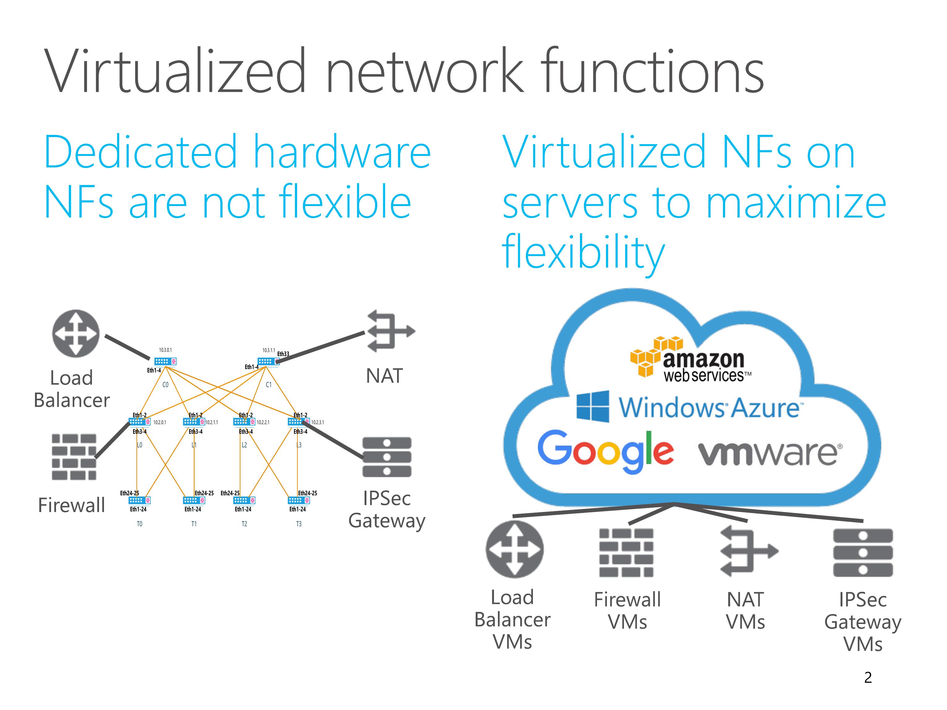
Multi-tenant datacenters requires flexible network functions to ensure security and performance isolation.
Dedicated hardware network function are not flexible enough to support multi-tenancy and respond to changing requirements.
Therefore, almost all cloud providers have been deploying virtualized network functions on servers to maximize flexibility.
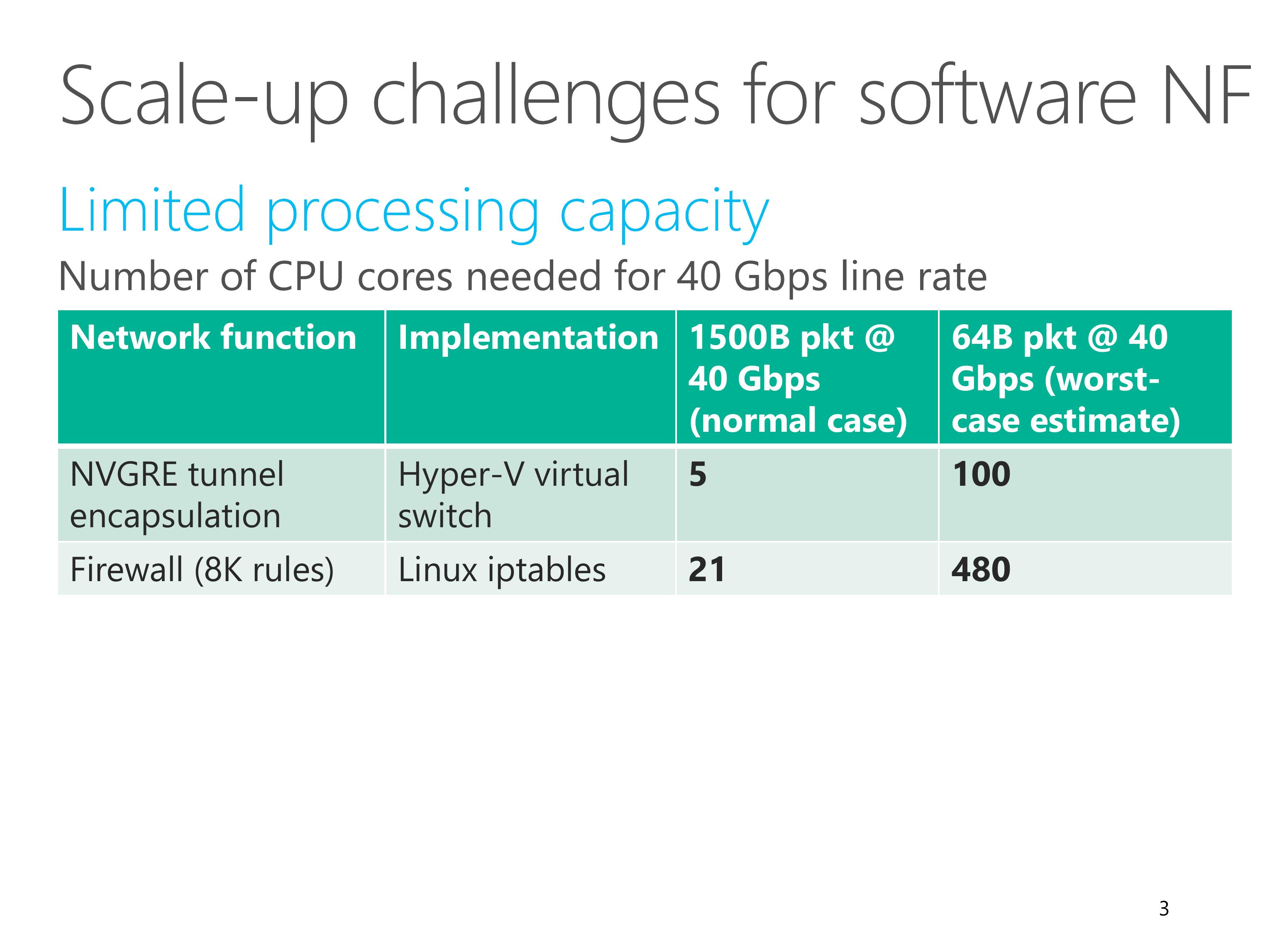
However, there are two major challenges for software network functions.
First, software network functions have limited processing capacity.
For example, for NVGRE tunnel encapsulation, the virtual switch requires 5 CPU cores to sustain 40 gigabit line rate.
In the worst case, when all the packets are tiny, it requires as many as 100 cores to sustain line rate.
This is only a rough estimation, but the order of magnitude should make sense.
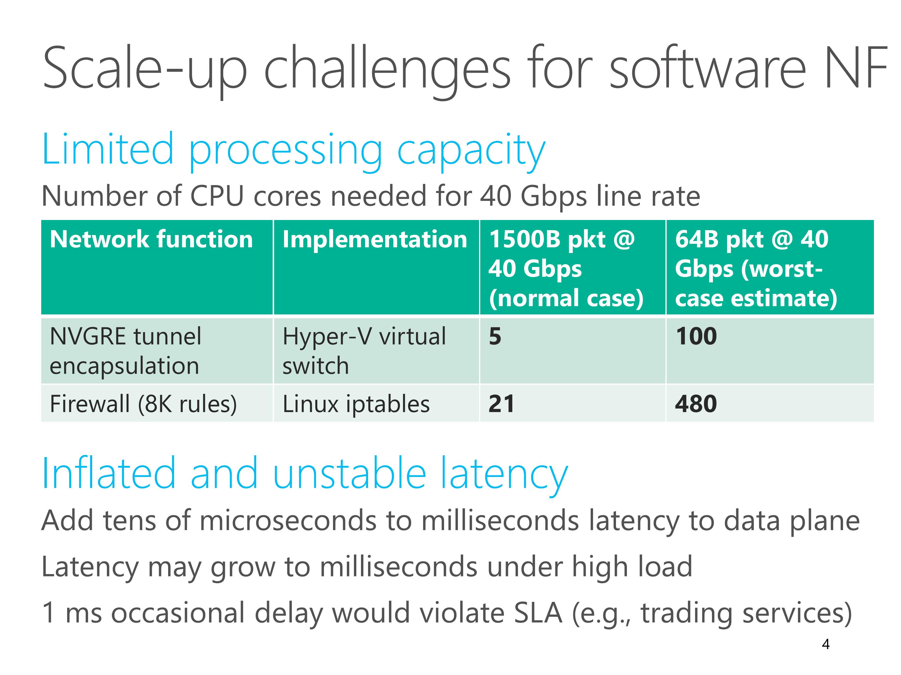
Second, software network functions have inflated and unstable latency.
A software-based network function adds tens of microseconds to milliseconds latency to the data plane.
When the load is high, this latency may grow to several milliseconds.
However, an occasional delay of one millisecond would already violate the service level agreement for delay sensitive applications.
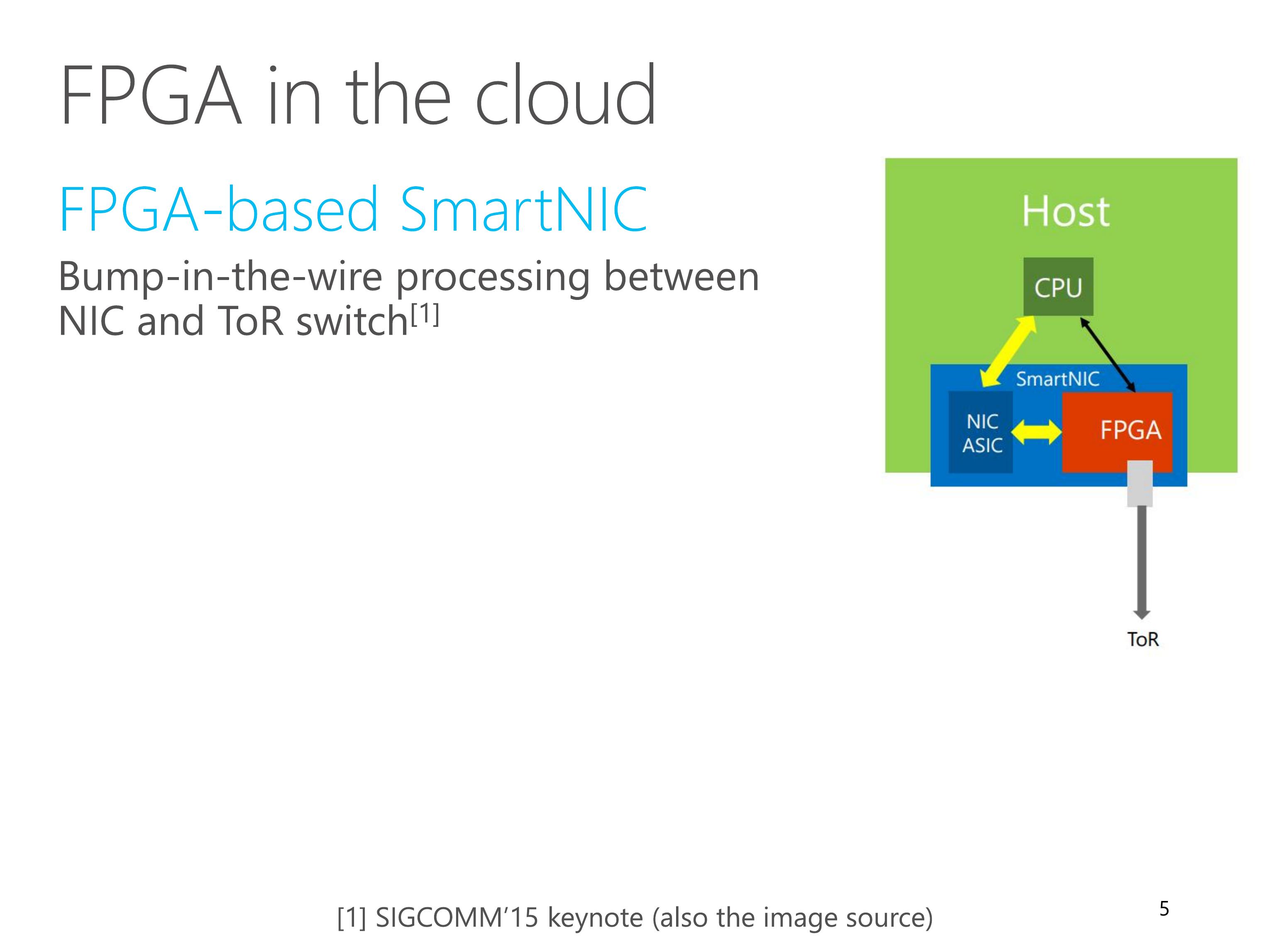
To accelerate network functions in servers, we have deployed FPGA-based SmartNICs at scale in Microsoft datacenters.
The FPGA performs bump-in-the-wire processing between commodity NIC and top-of-rack switch.
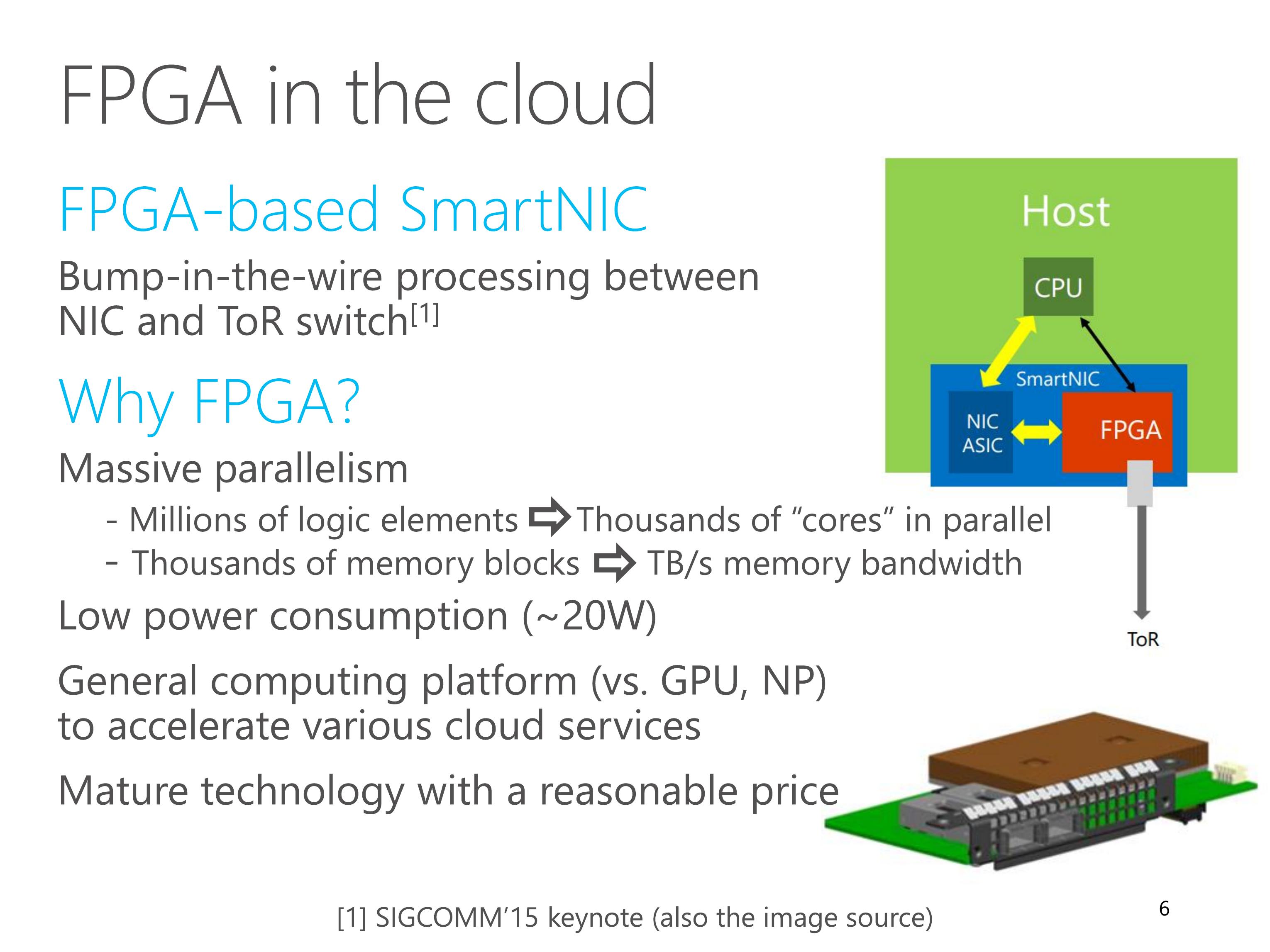
There are several reasons for choosing FPGA as the accelerator.
First, FPGA has massive parallelism.
It has millions of logic elements, which can build thousands of “cores” running in parallel.
FPGA also has thousands of memory blocks, which can produce terabytes per second aggregated memory bandwidth.
Second, FPGA has low power utilization.
Third, FPGA is a general computing platform to accelerate various cloud services, for example Bing search ranking.
Finally, FPGA is a mature technology with reasonable price in recent years.
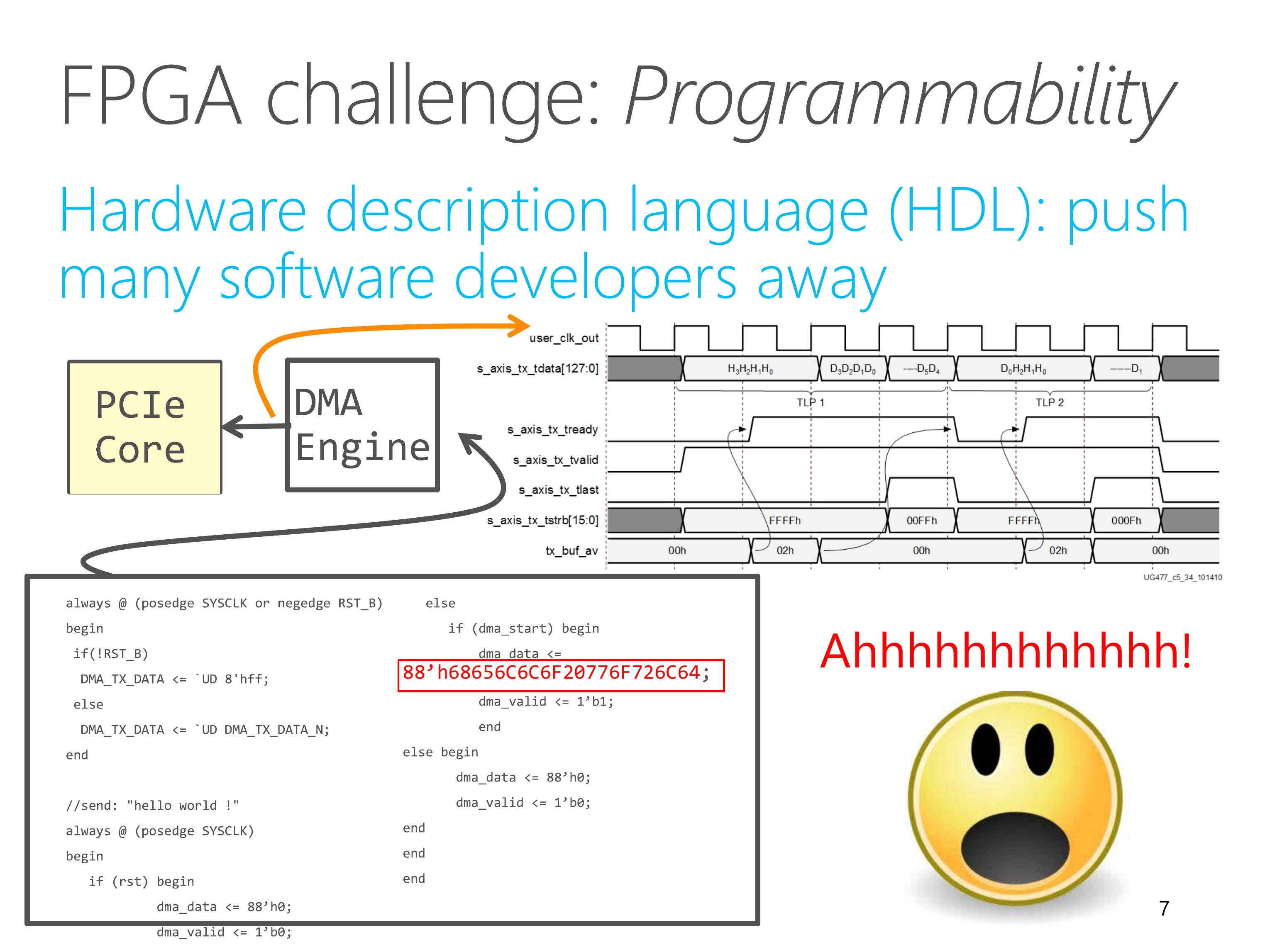
The main challenge to use FPGA is programmability.
Conventionally, FPGA is programmed with low-level hardware description languages, such as Verilog and VHDL.
This example shows a HelloWorld program in Verilog.
To print a HelloWorld string on the screen, we first need to translate the string into ASCII codes.
In order to send the codes to the host memory, we need to write a DMA engine.
The DMA engine needs to call a PCI express IP core, which requires reading three hundred pages of manual to understand the interface.
The difficulty of hardware description languages have pushed many software developers away for years.
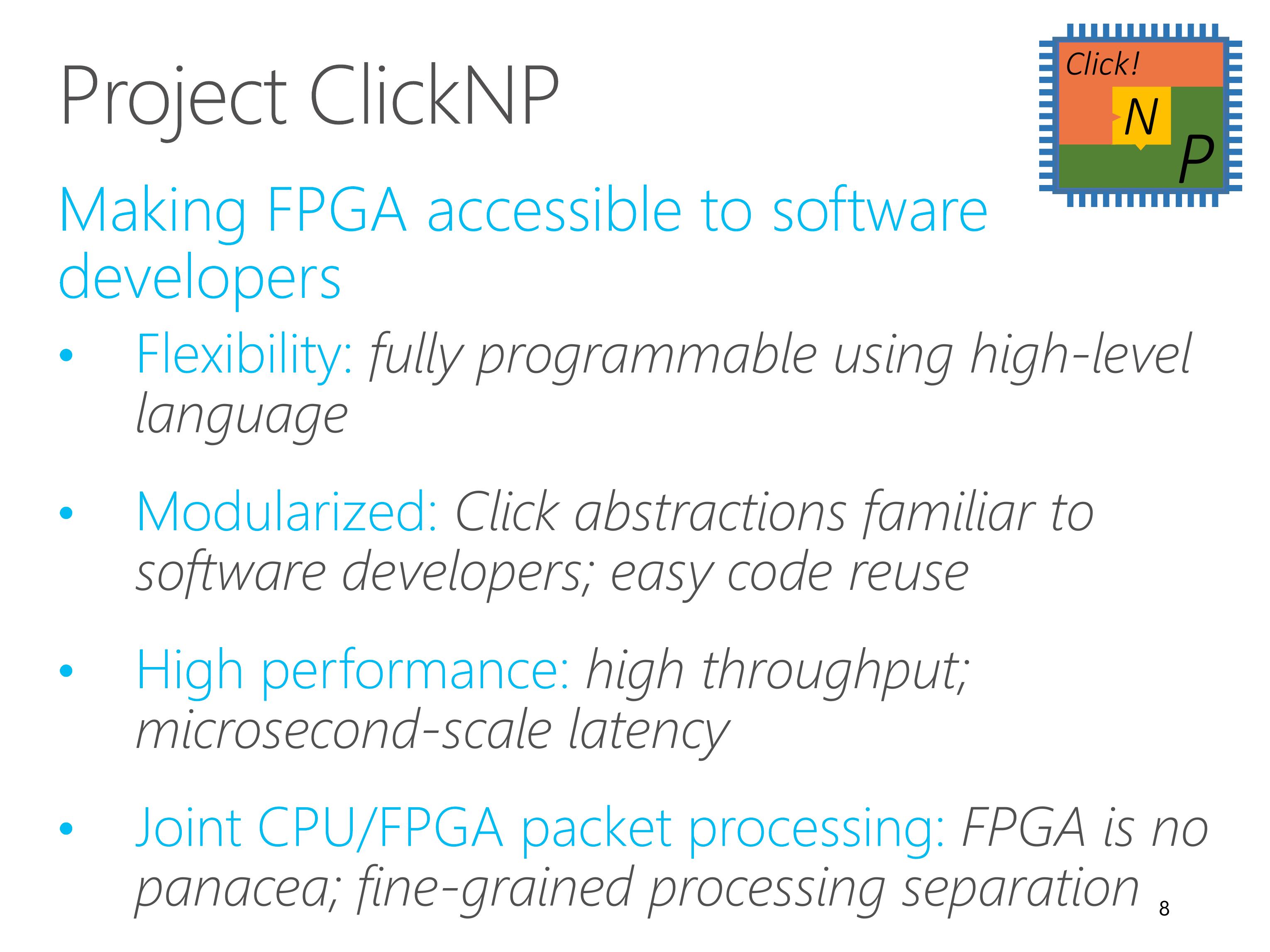
In this work, we present ClickNP, a platform to make FPGA accessible to software developers.
We have several design goals.
First, the platform should be fully programmable using high-level languages.
Second, the platform should have a modular architecture familiar to software developers. In particular, we choose abstractions similar to the Click modular router for easy code reuse.
Third, the platform should provide high performance, both in terms of throughput and latency.
Finally, the platform should support joint CPU and FPGA packet processing. That’s because FPGA is not suitable for every kind of workload. We should support fine-grained processing separation between CPU and FPGA. This requires high performance and low latency communication between CPU and FPGA.
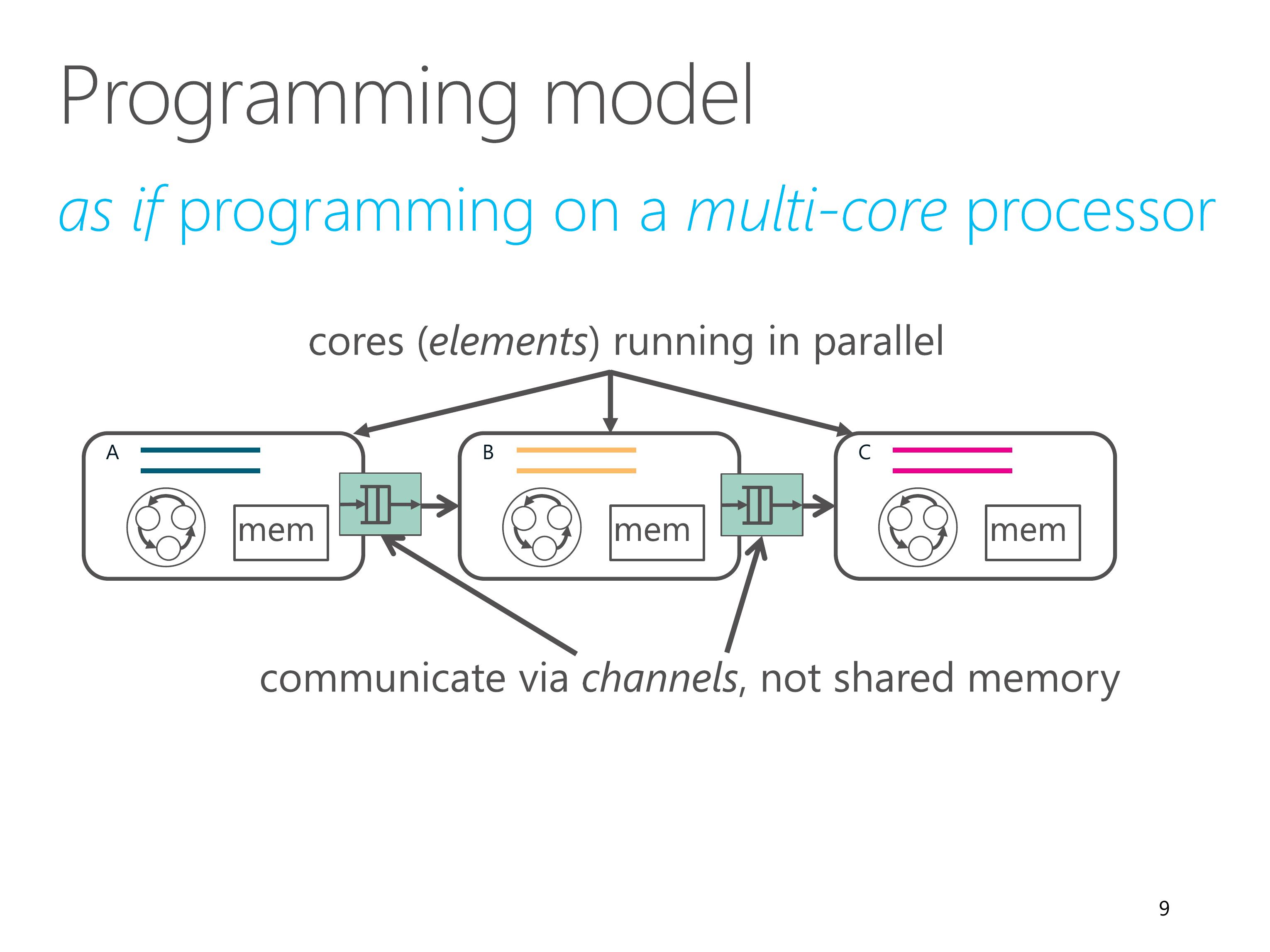
ClickNP provides a modular programming model similar to the Click modular router.
Therefore, programming in ClickNP is much like programming on a multi-core processor.
There is one important difference, though.
In conventional multi-core processing, threads communicate via shared memory.
However, In ClickNP, the cores communicate via channels instead of shared memory.
Channel-based communication is more efficient in FPGA compared to shared global memory, because the shared global memory would be the bottleneck.
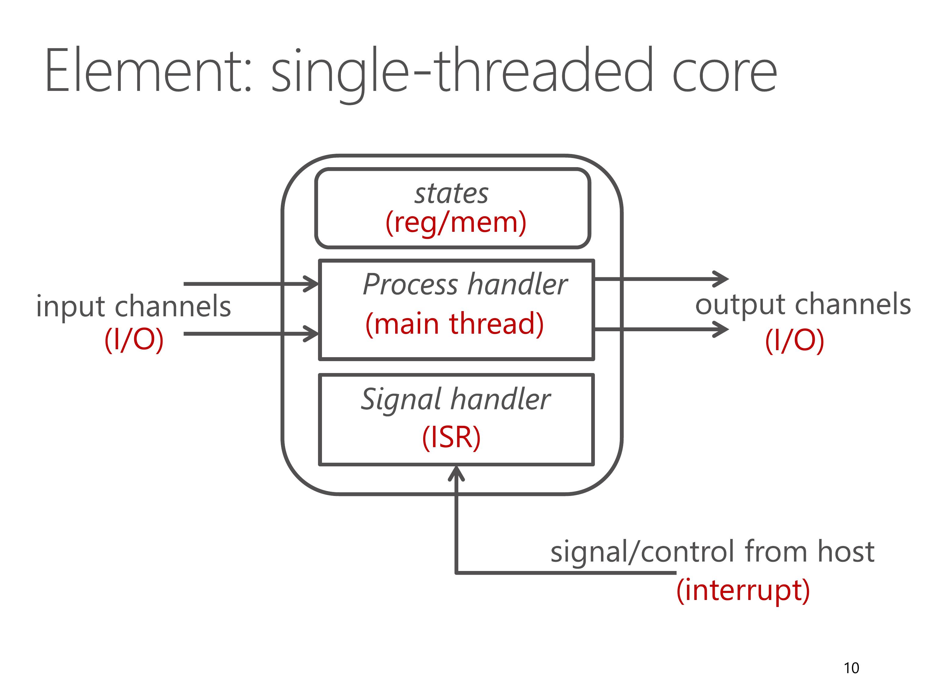
In ClickNP, the basic processing module is called an element, which resembles a single-threaded core.
Each element has the following components.
First, a set of local states that are only accessible inside the element.
Second, input and output channels to communicate with other elements.
Third, process handler, which is the main thread to read input channels, do processing and write to output channels in an infinite loop.
Finally, signal handler, which receives and processes commands from the manager thread in host program running on CPU. Signals resemble interrupts in CPU.
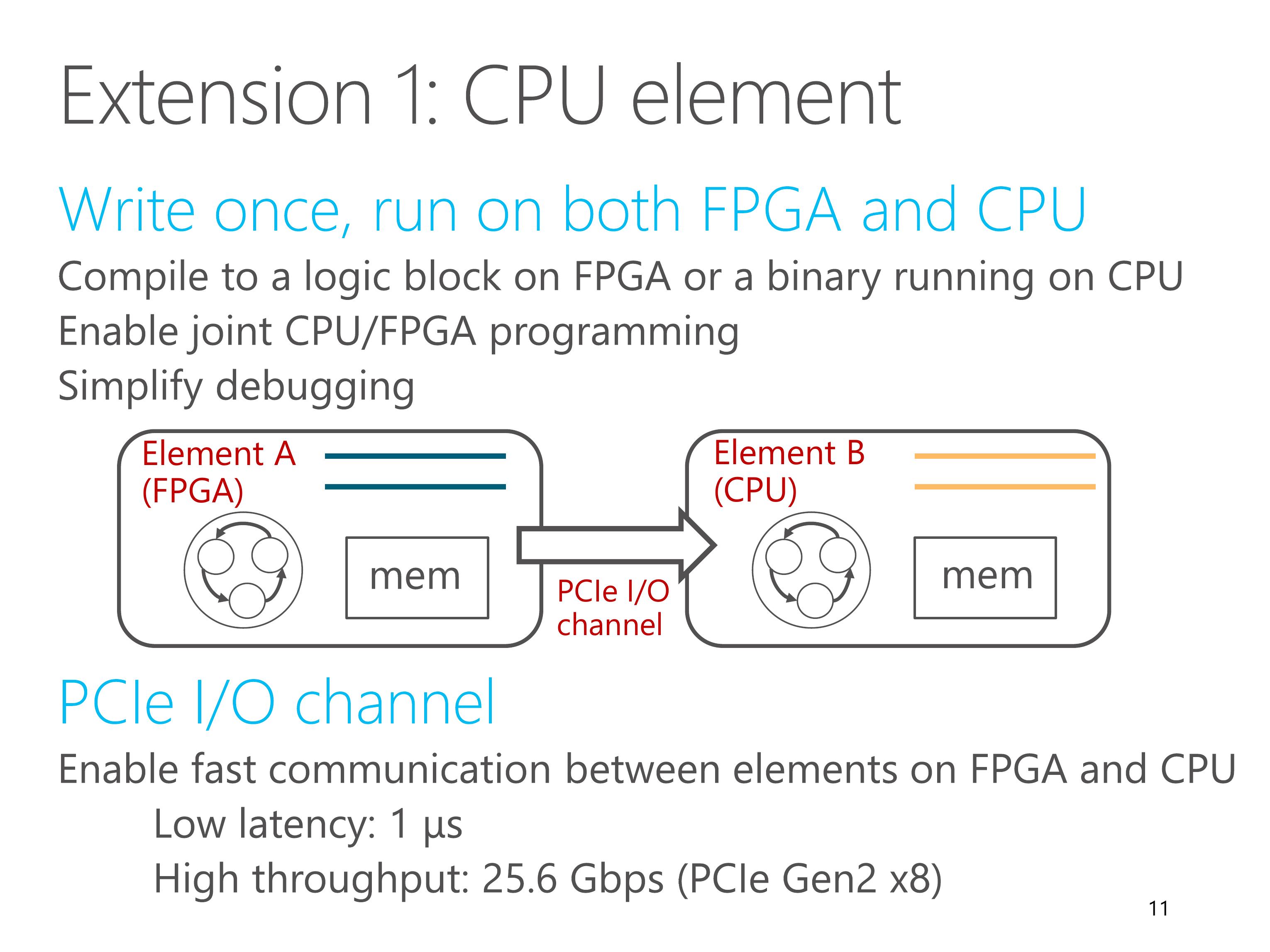
Because elements are written in C language, they can run on both FPGA and CPU.
Each element can be configured to compile to a logic block on FPGA, or compile to a thread running on CPU.
CPU elements enable joint CPU/FPGA programming and simplifies debugging. We can debug the elements with familiar debugging tools on CPU.
FPGA elements communicate with CPU elements via PCIe I/O channel.
It enables low latency and high throughput communication between elements on FPGA and CPU.
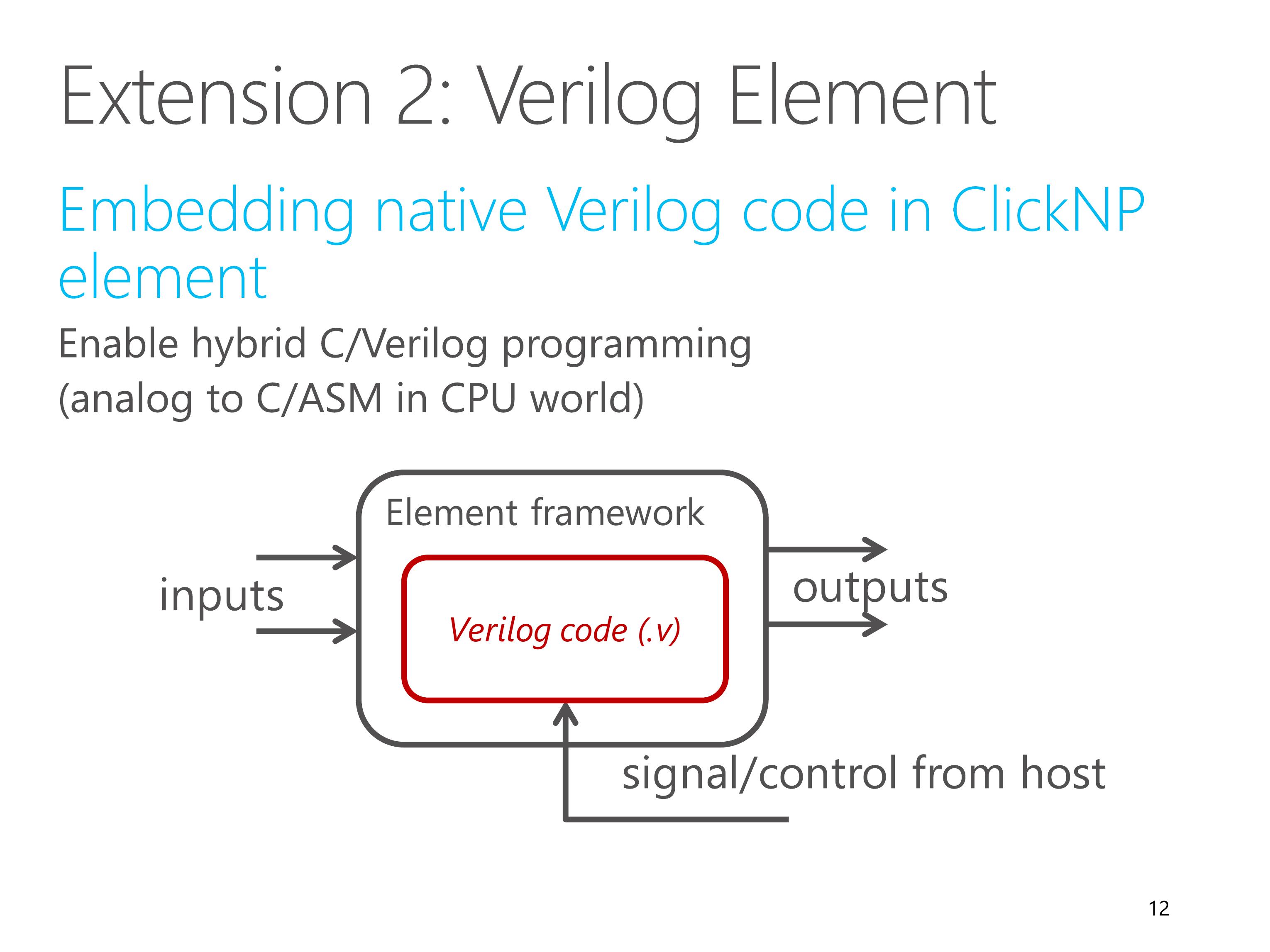
A second extension to the element abstraction is Verilog element.
This is not in the paper, but current ClickNP also support that.
Verilog element enables hybrid C and Verilog programming, which is similar to C and assembly in CPU world.
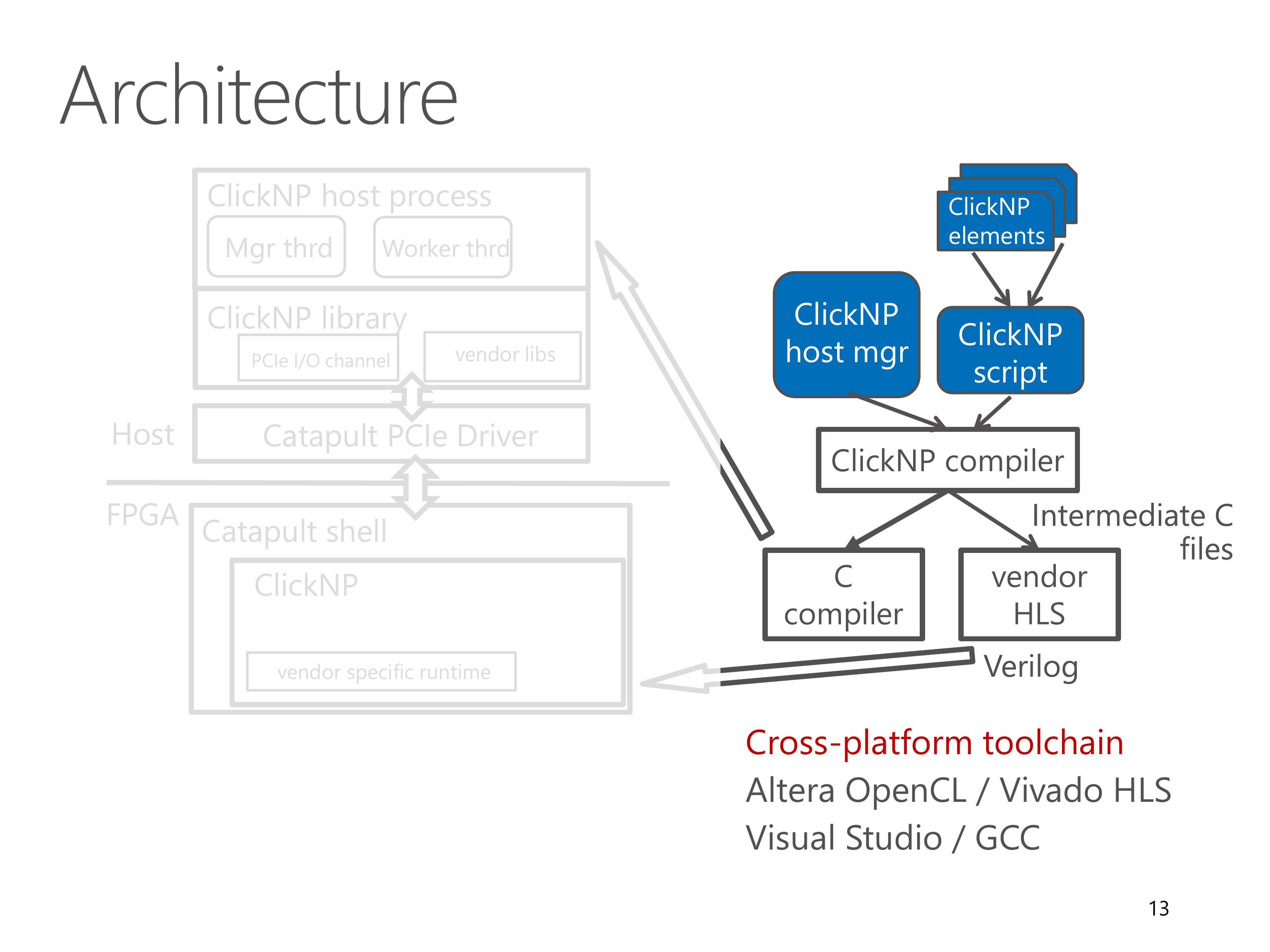
Here we look at the architecture of the ClickNP toolchain.
A ClickNP program is divided into three parts, a set of ClickNP elements, a ClickNP script to define the connections among elements, and a ClickNP host manager program.
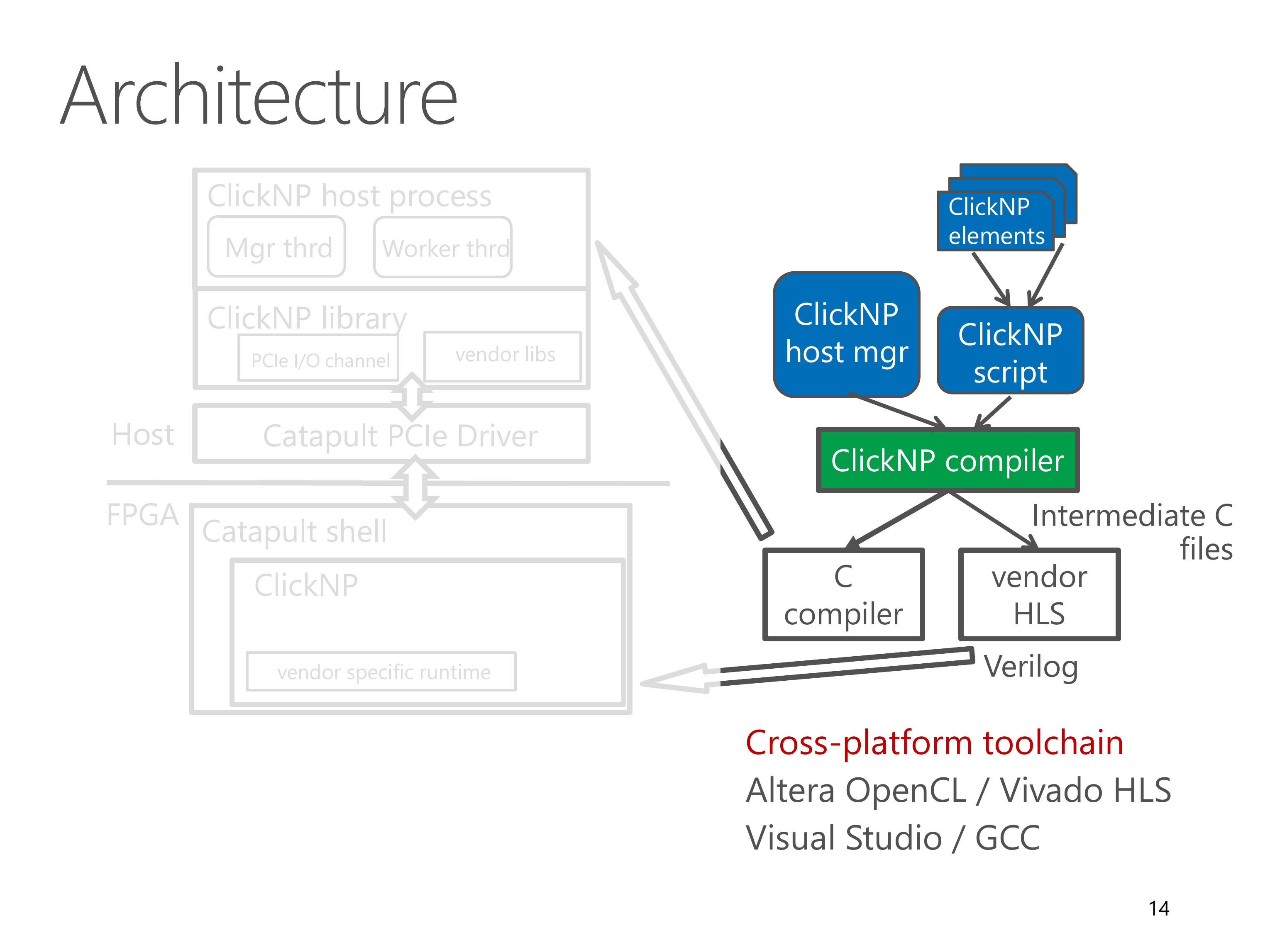
The ClickNP compiler first compiles the ClickNP program to intermediate C code.
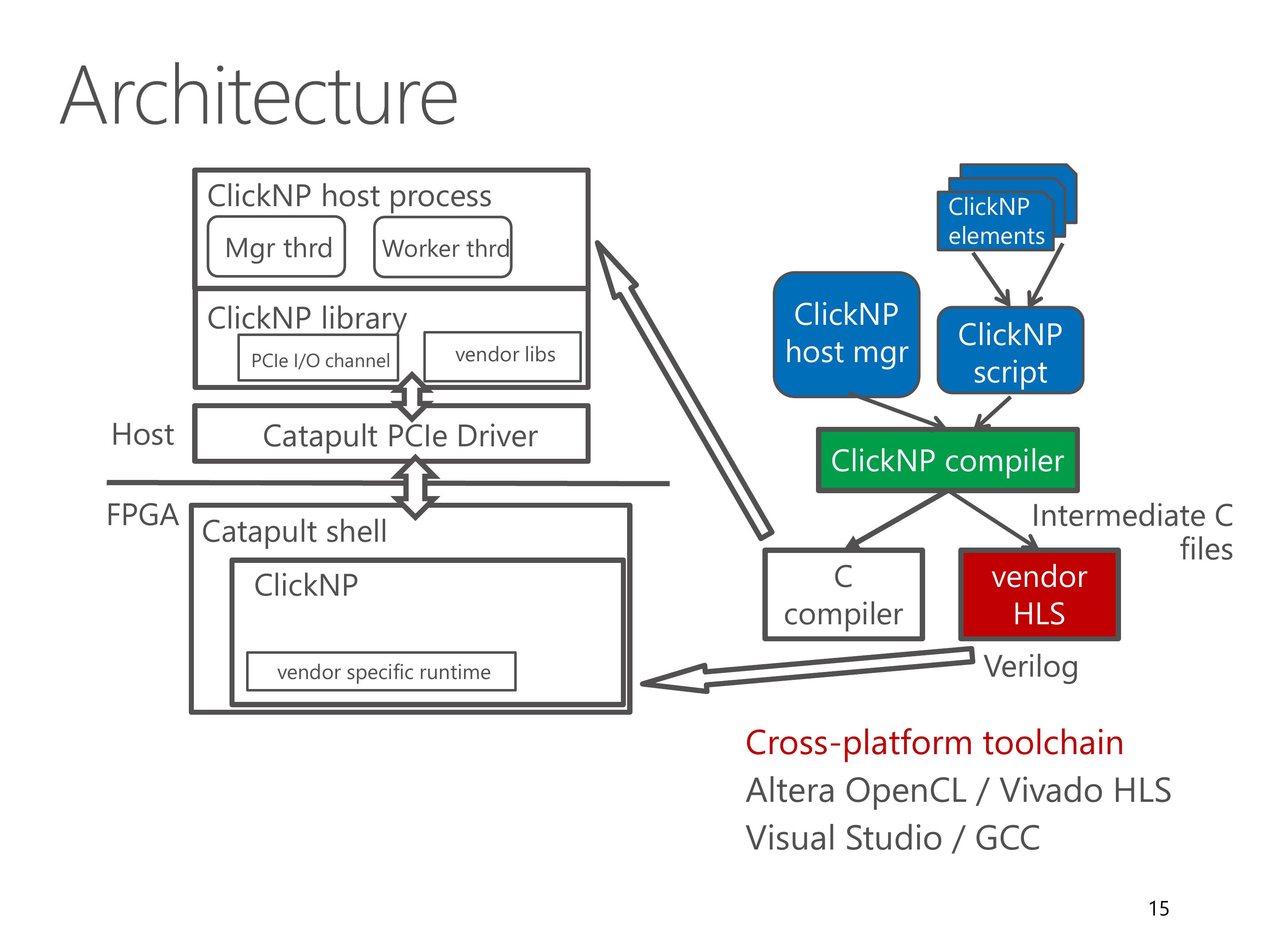
Then we invoke a vendor HLS tool, for example Altera OpenCL or Vivado HLS, to compile the intermediate C code into Verilog code.
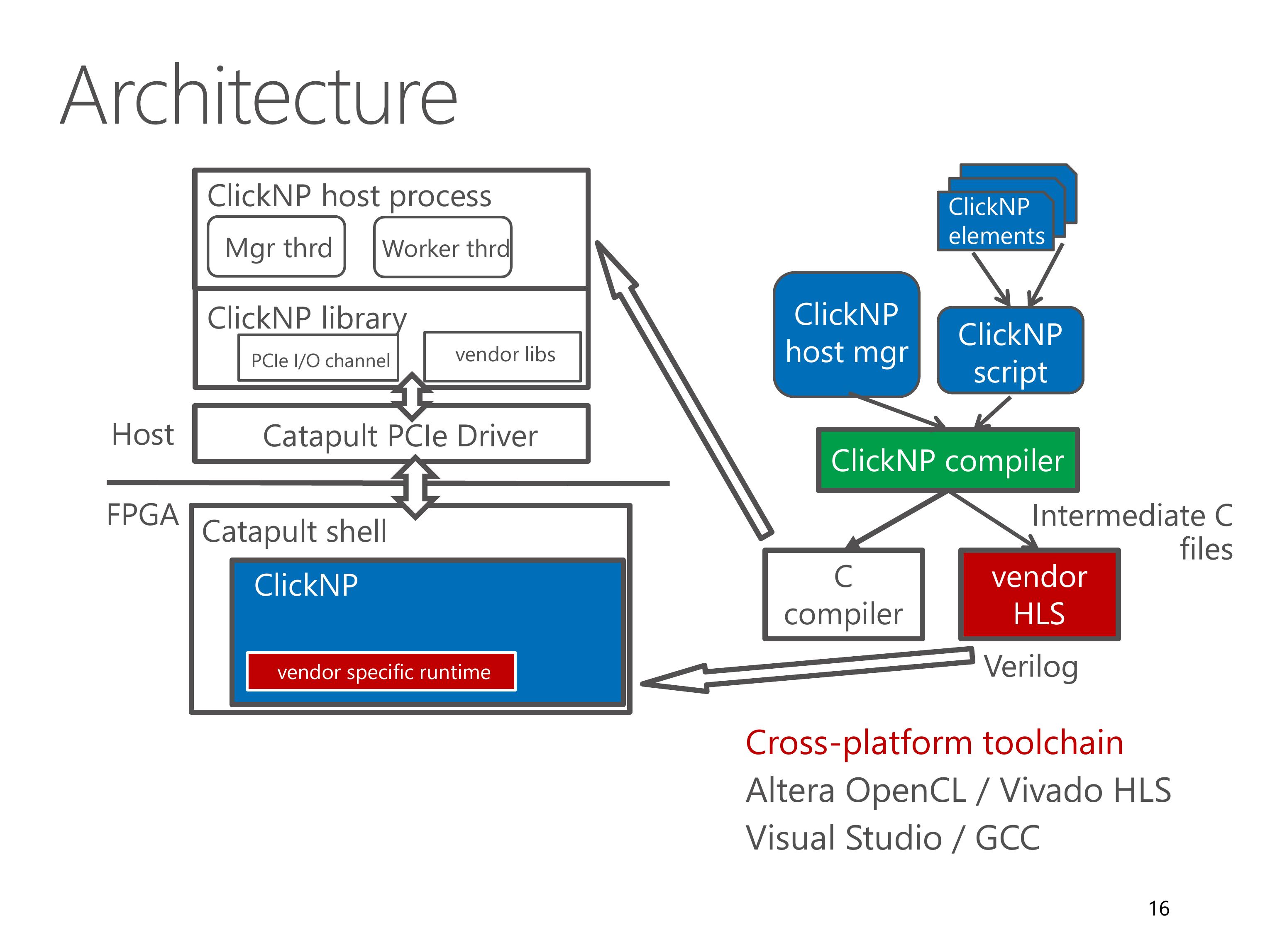
Finally we call the hardware synthesis toolchain to generate the FPGA bitstream.
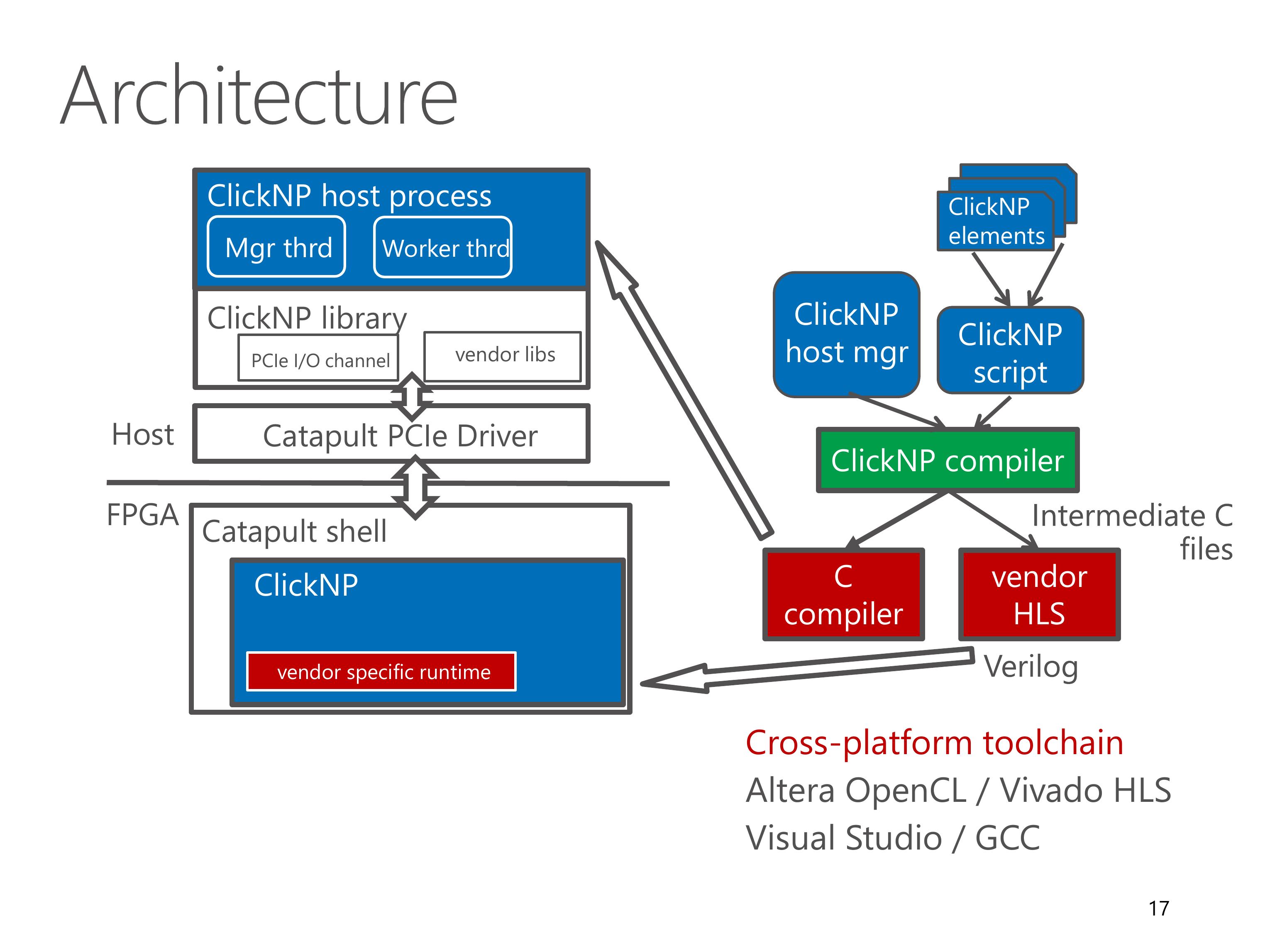
And call a standard C compiler to compile the ClickNP host program.
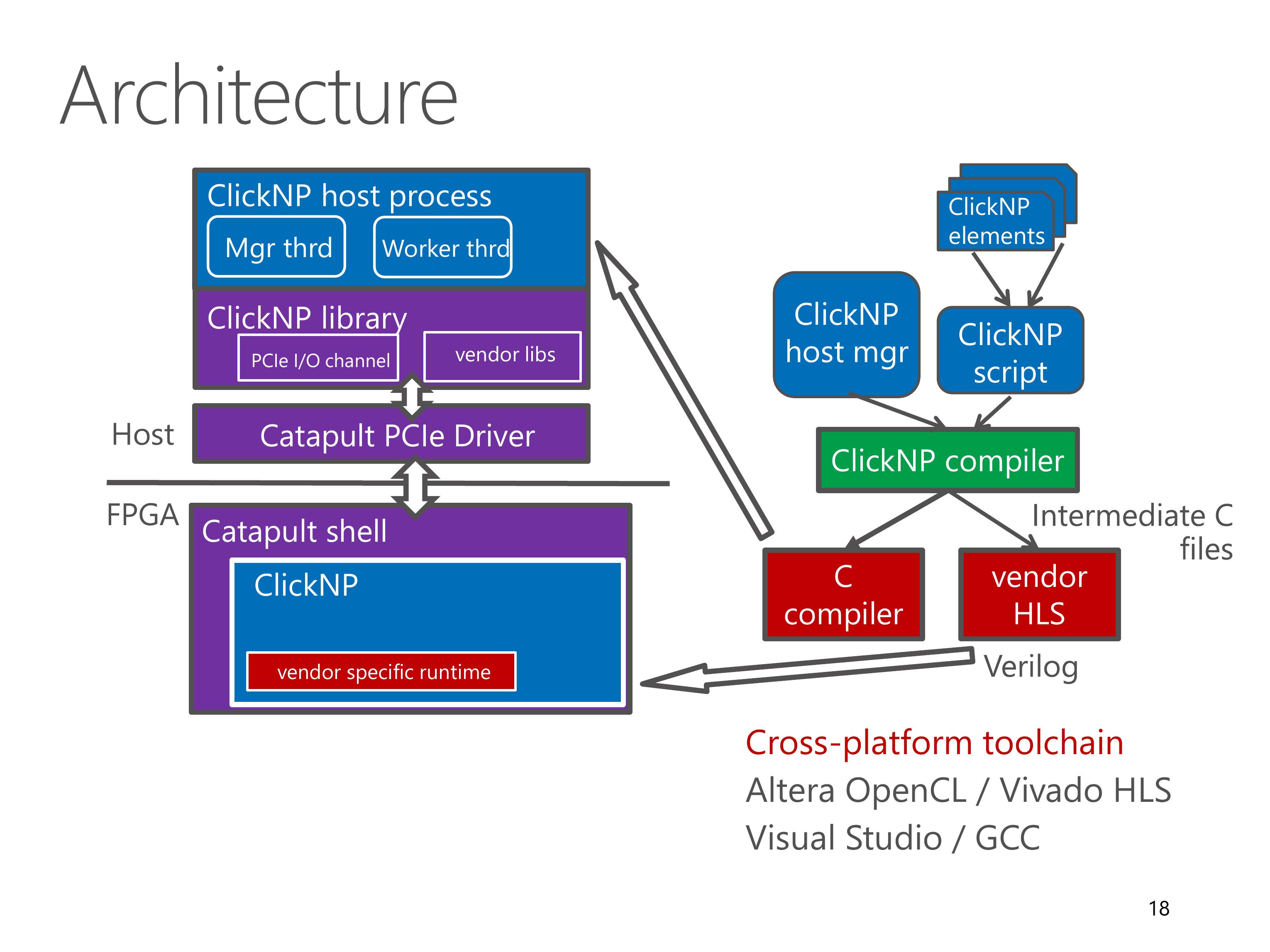
In runtime environment, the Catapult shell is the operating system on the FPGA, which was developed by the Microsoft Catapult team.
The Catapult shell provides resource abstractions to the ClickNP application logic.
On host side, the ClickNP library provides PCIe I/O channel abstraction to the CPU elements, and enables the host program to communicate with FPGA elements via signals.
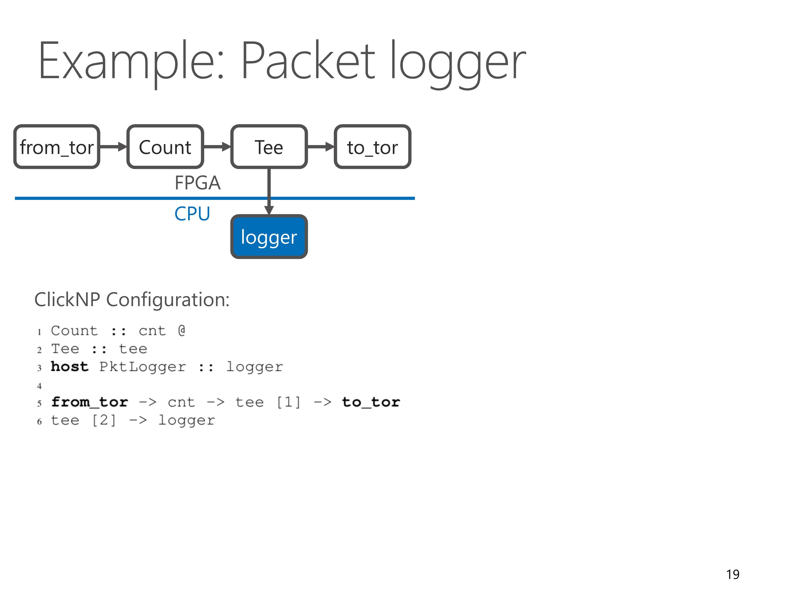
Here we look at an example network function, packet logger.
It receives packets from top-of-rack switch, counts number of packets in Count element, then makes a copy in Tee element.
One copy is forwarded back to ToR switch, the other copy is forwarded to a host element PktLogger running on CPU.
We can see that this PacketLogger needs only 5 lines of code for ClickNP configuration.
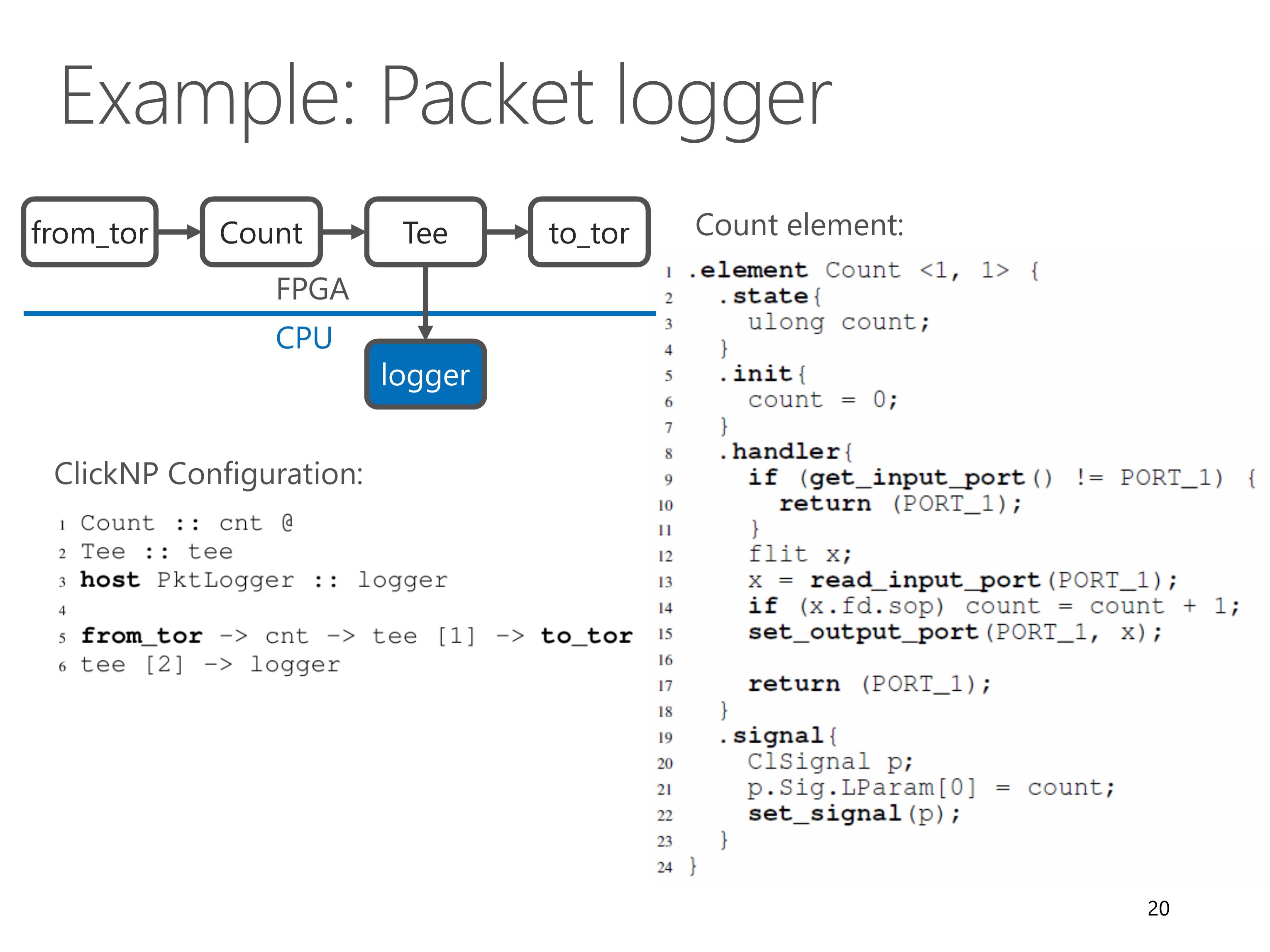
Now we look at details of the Count element.
The first line of code shows that the Count element has one input channel and one output channel.
There is only one state variable, count, and initialized to zero.
In the handler, we first check whether or not the input channel has data to read. If so, we read a block of packet data from the input channel.
If the metadata indicates that it is start of packet, we increment the counter by one.
Finally we forward the data to the output port.
The signal handler simply writes the counter to a special structure called ClSignal, which is then returned to the manager thread in host program.
Now we come to optimizations in ClickNP.
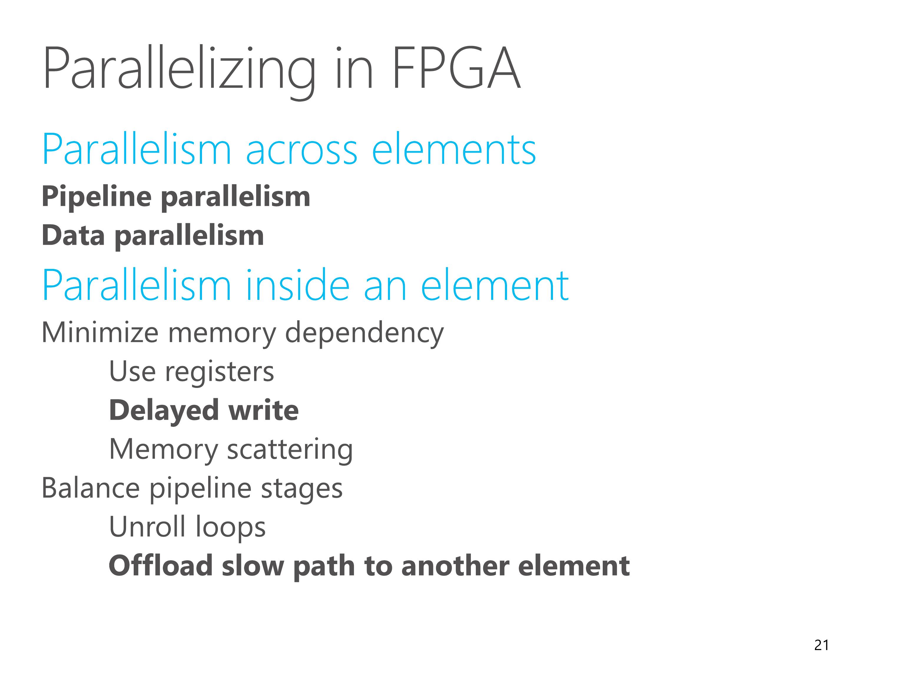
As we know, efficient FPGA code must utilize parallelism, which basically includes parallelism across elements and parallelism inside an element.
Due to time limitations, here I’m only going to discuss several of them. For the remaining ones, please refer to the paper.
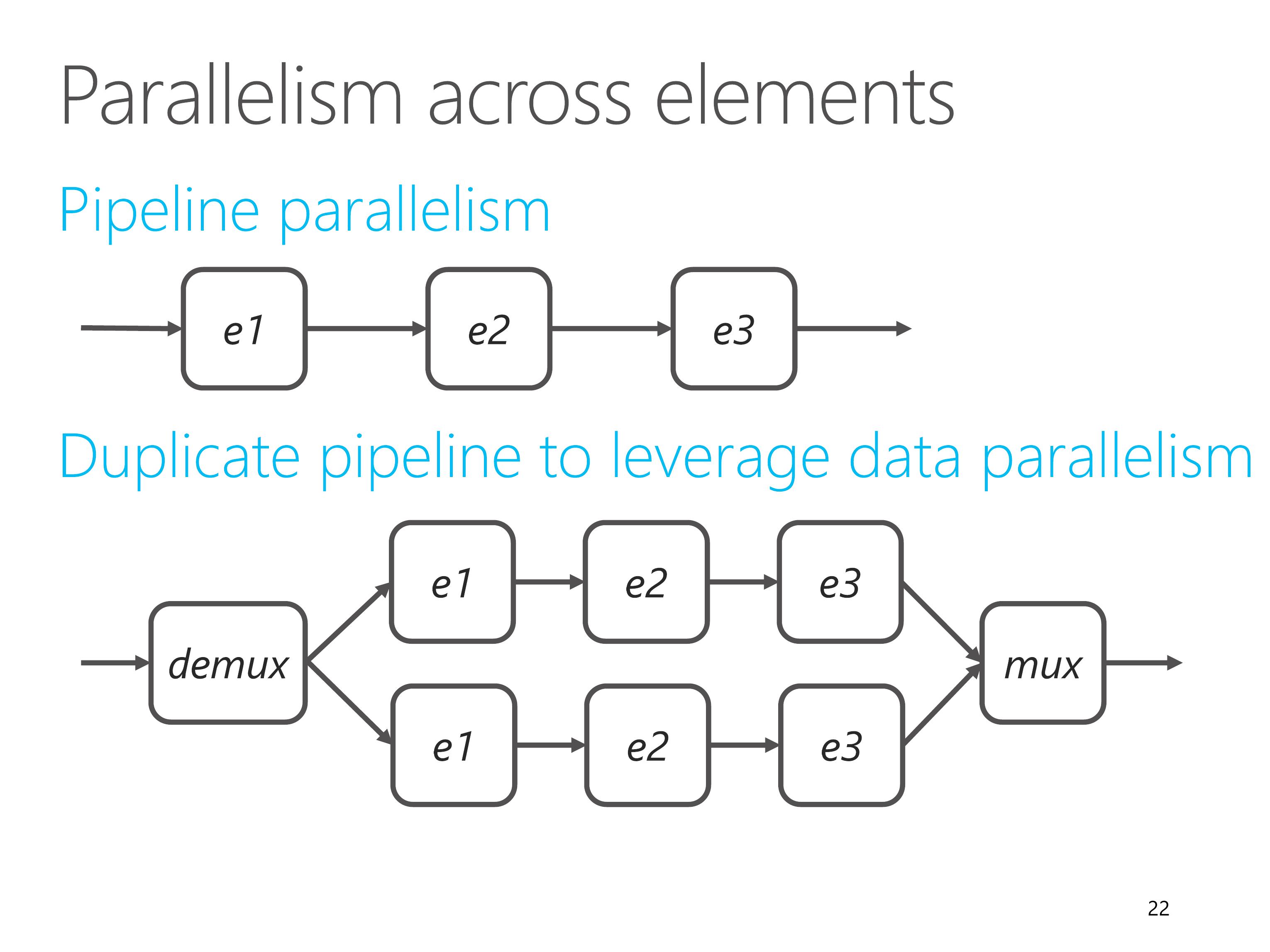
First, parallelism across elements.
In ClickNP, packets flow from one element to another via a processing pipeline. Different pipeline stages, which means different elements, are processing different data in parallel. This is called pipeline parallelism.
If a single pipeline cannot sustain the required throughput, we can duplicate the pipeline to leverage data parallelism.
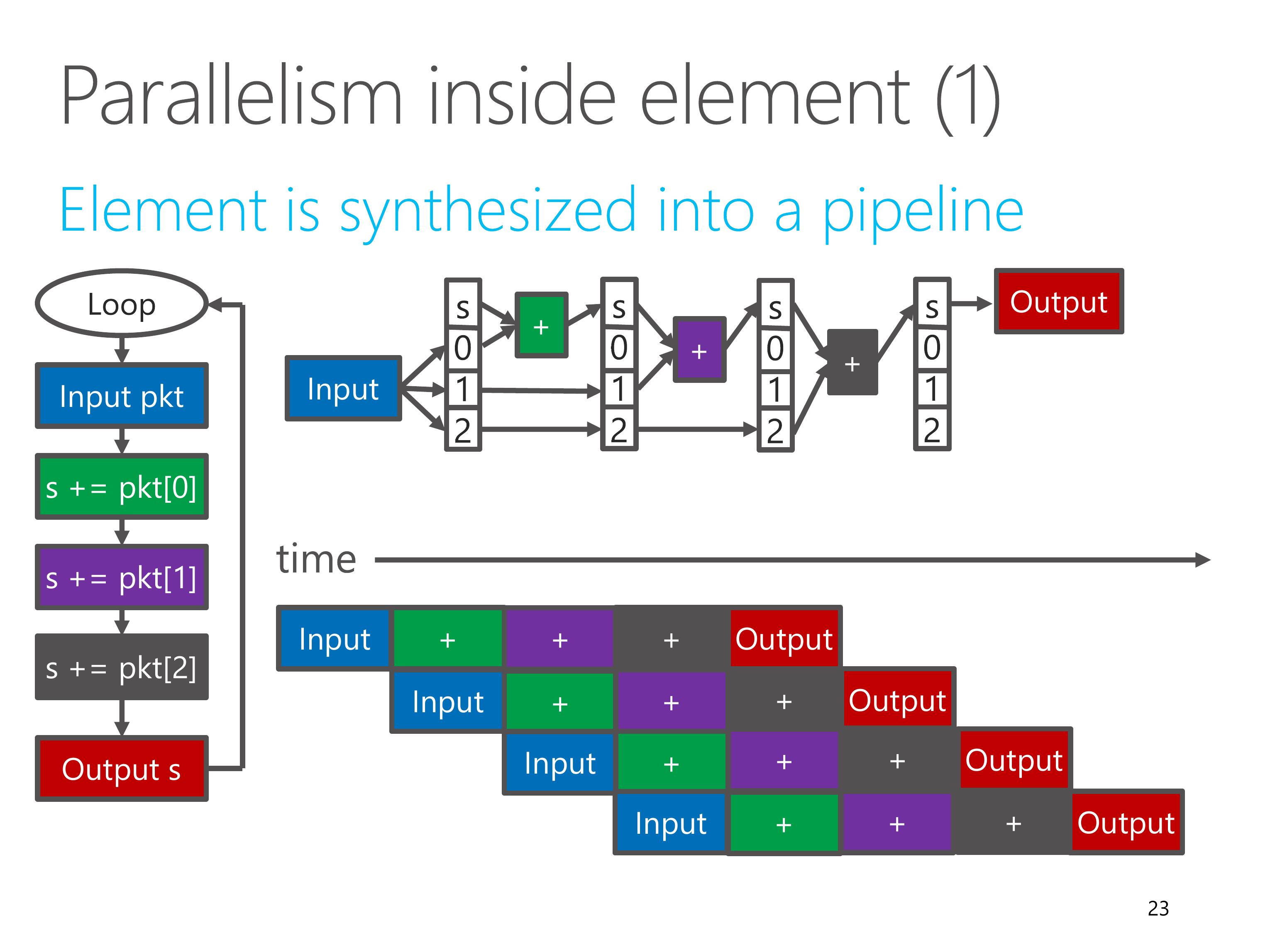
Next, parallelism inside element.
In ClickNP, each element is synthesized into a processing pipeline.
Different pipeline stages are processing different data in parallel.
Every clock cycle, one input datum is read, each pipeline stage moves to the next stage, and one output datum is written.
So the throughput is one datum per clock cycle.
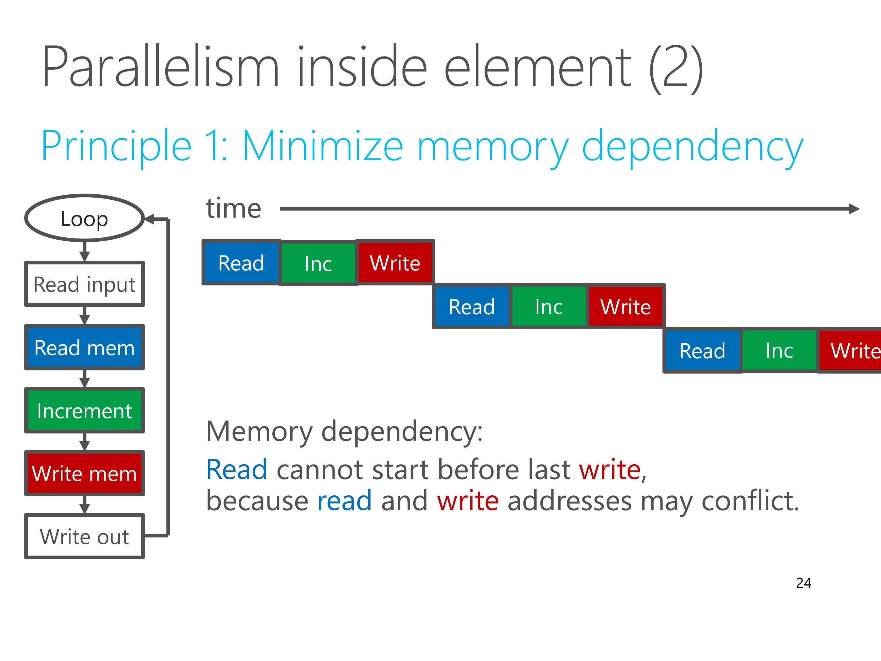
However, this efficient pipeline processing could break in several situations.
First, when there is memory dependency.
This example shows a most common case of memory dependency, the read-write dependency.
If the read and write operation accesses the same memory block, the read operation cannot start before last write operation, because read and write addresses may conflict.
Our principle is to minimize memory dependency.
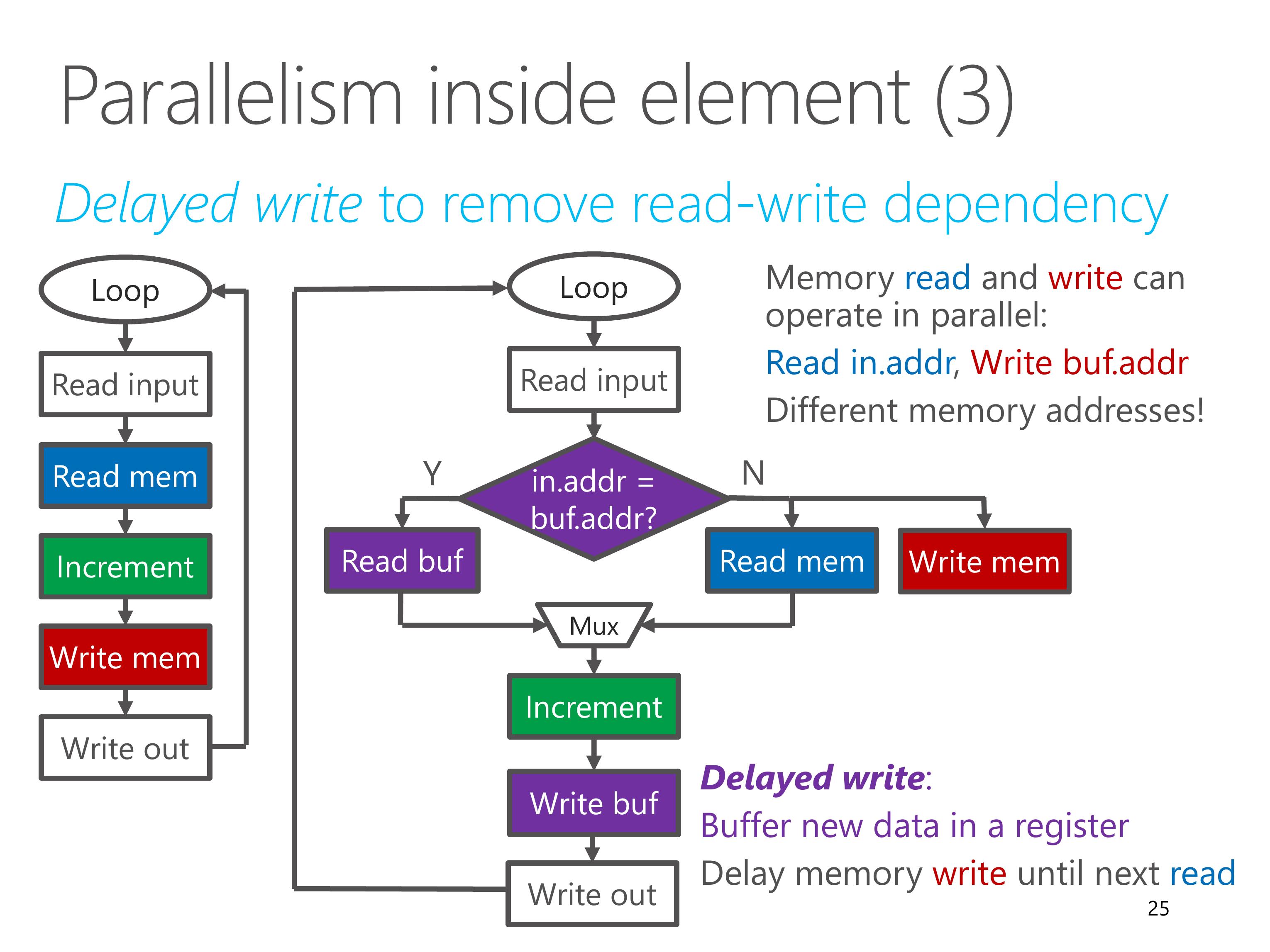
To resolve the read-write memory dependency, we use a technique called delayed write.
We buffer the new data in a register, and delay the memory write operation until the next read operation.
If the next read operation accesses the same memory address, we read the value from the buffer register directly.
Otherwise, the memory read and memory write can operate in parallel, because they access different memory addresses.
The ClickNP compiler can perform this delayed write optimization automatically.
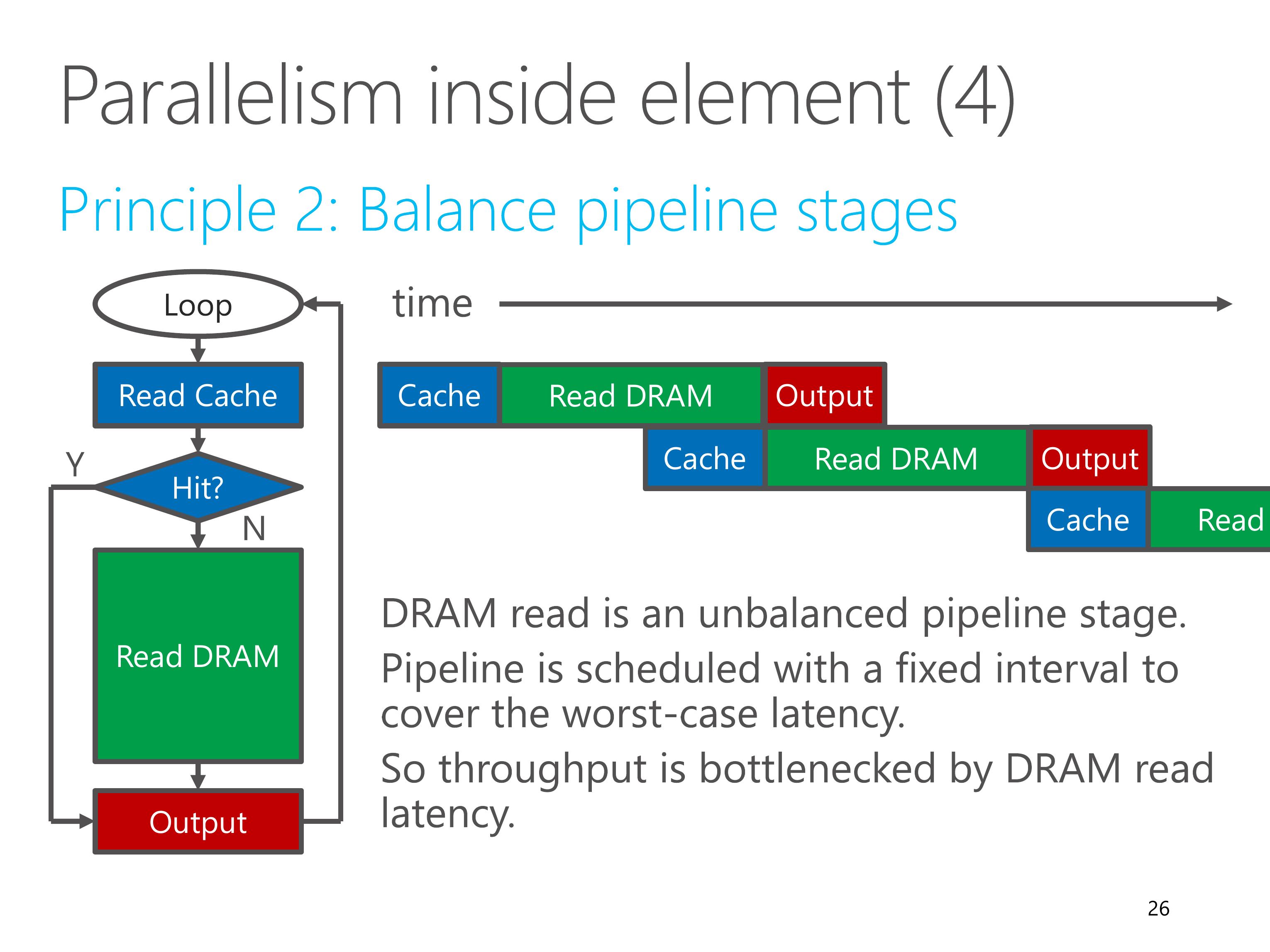
Except for memory dependency, another source of inefficiency in elements is unbalanced pipeline stages.
In this example, we first lookup the cache, if cache hit, directly output, if cache miss, then lookup the DRAM.
DRAM read has high latency, which is an unbalanced pipeline stage.
However, the pipeline is scheduled with a fixed interval to cover the worst-case latency.
So the throughput of the element is therefore bottlenecked by the DRAM read latency.
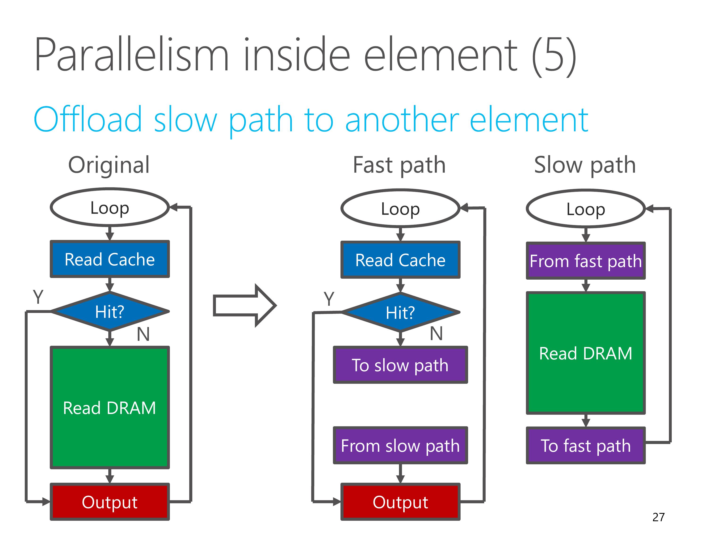
In this case, our solution is to offload the slow path to another element.
We move the “Read DRAM” part to another element called slow path.
The fast path element and slow path element are coordinated via channels.
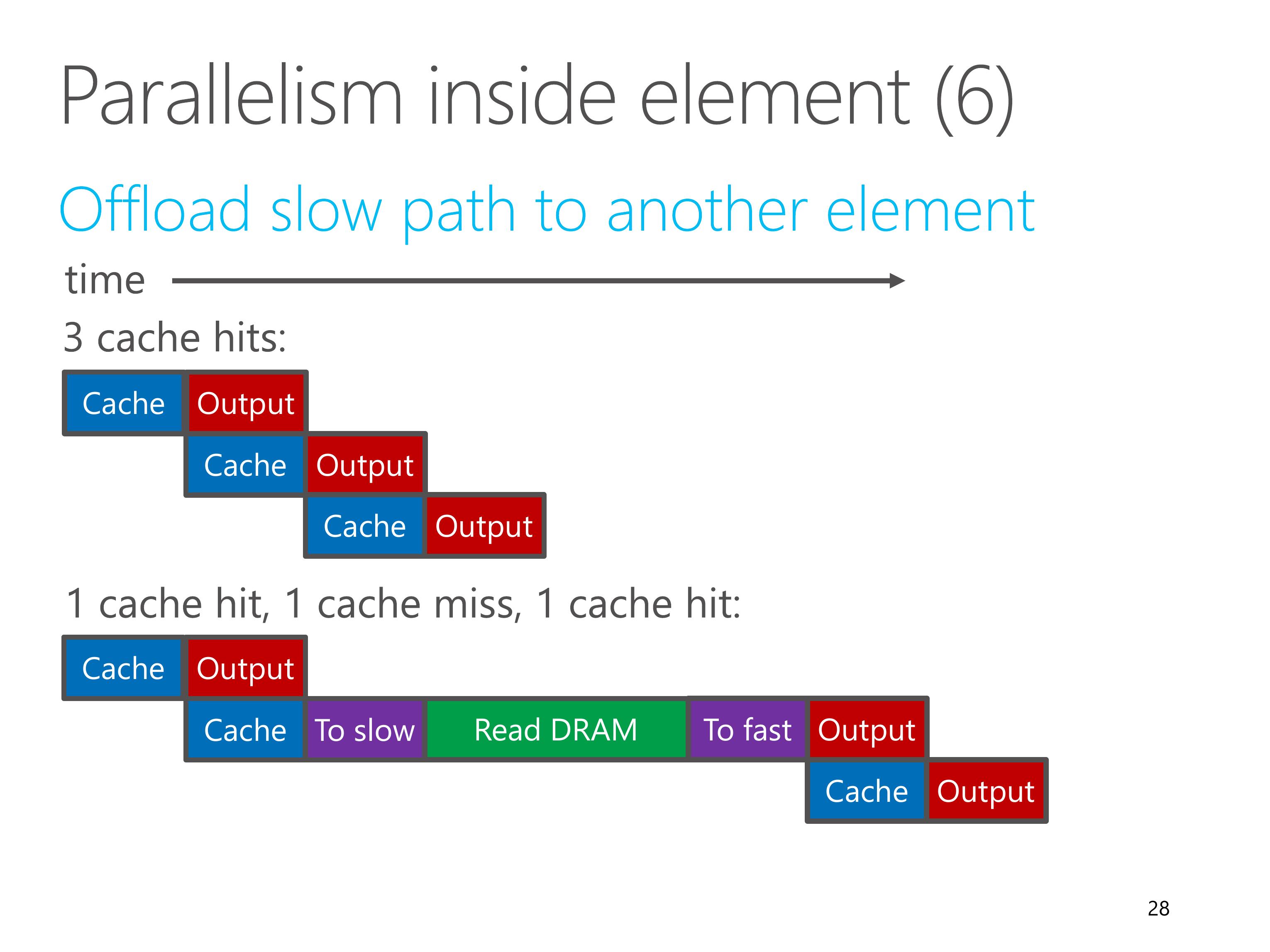
After offloading, the fast path is no longer bottlenecked by the DRAM read.
If all packets hit the cache, then the fast path can process one packet per clock cycle.
If a packet is cache miss, then the fast path needs to wait for the slow path to read the DRAM.
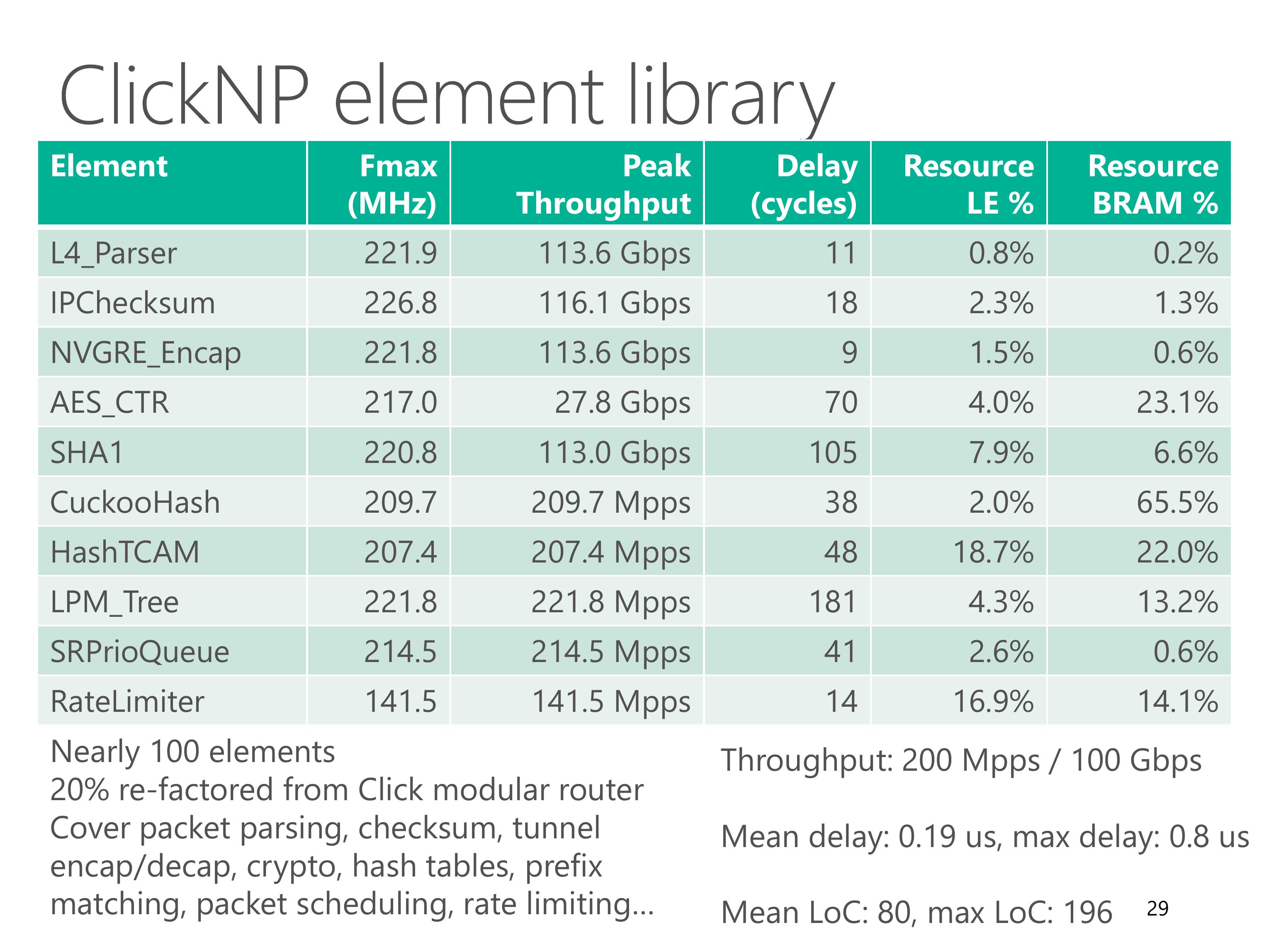
We have built a ClickNP element library with nearly 100 elements.
About 20% of them are re-factored from Click modular router, and the remaining ones cover lots of network functions.
This table shows some common elements in the element library, which cover packet parsing, checksum, tunnel encapsulation, crypto, hash tables, prefix matching, packet scheduling and rate limiting.

Leveraging the optimization techniques we just discussed, each element can achieve high throughput.
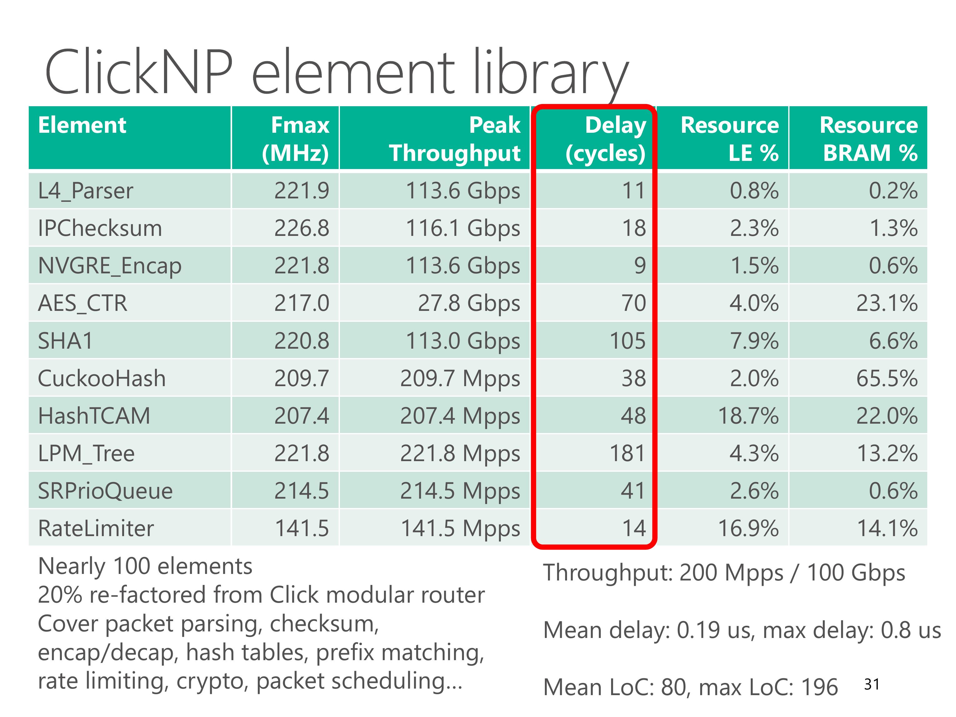
The delay of each element is also low. The maximum delay is below 1 microsecond.
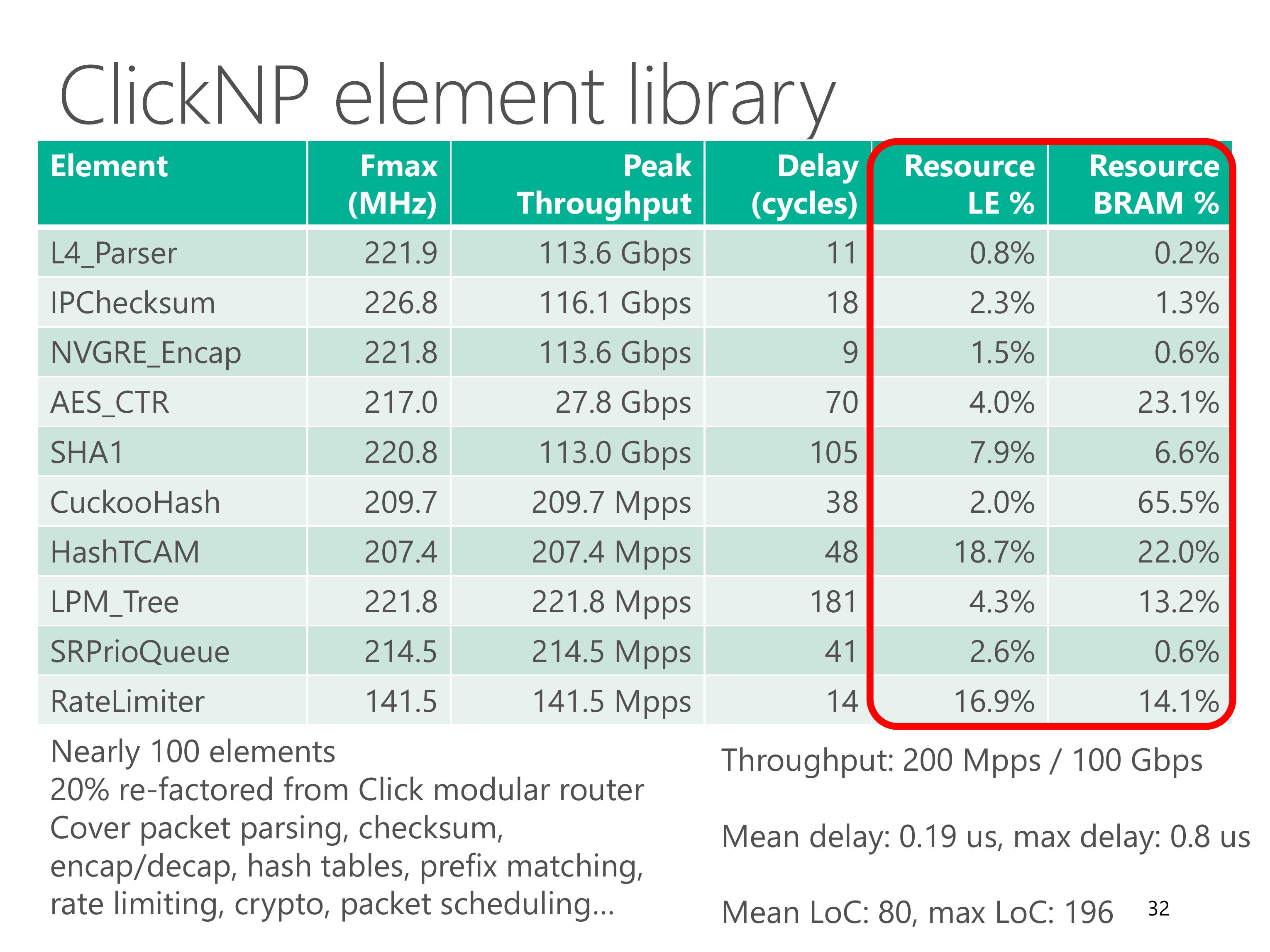
Resource utilization of each element is also modest.
The BRAM usage typically depends on element configuration, for example flow table size.
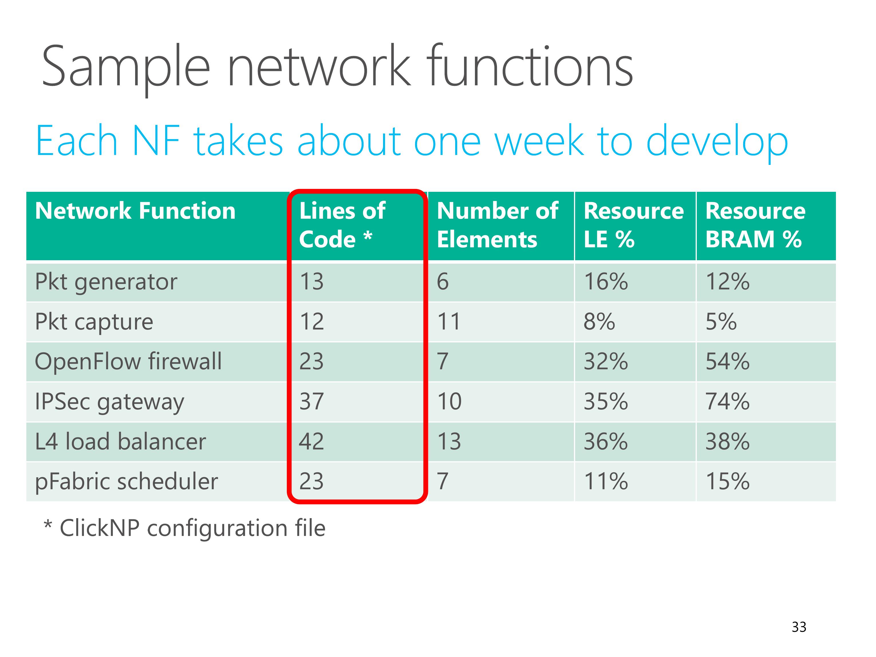
Using the 100 elements in ClickNP, we have built several sample network functions.
Each network function only needs tens of lines of code for the ClickNP configuration file.
Each network function only takes about one week to develop.
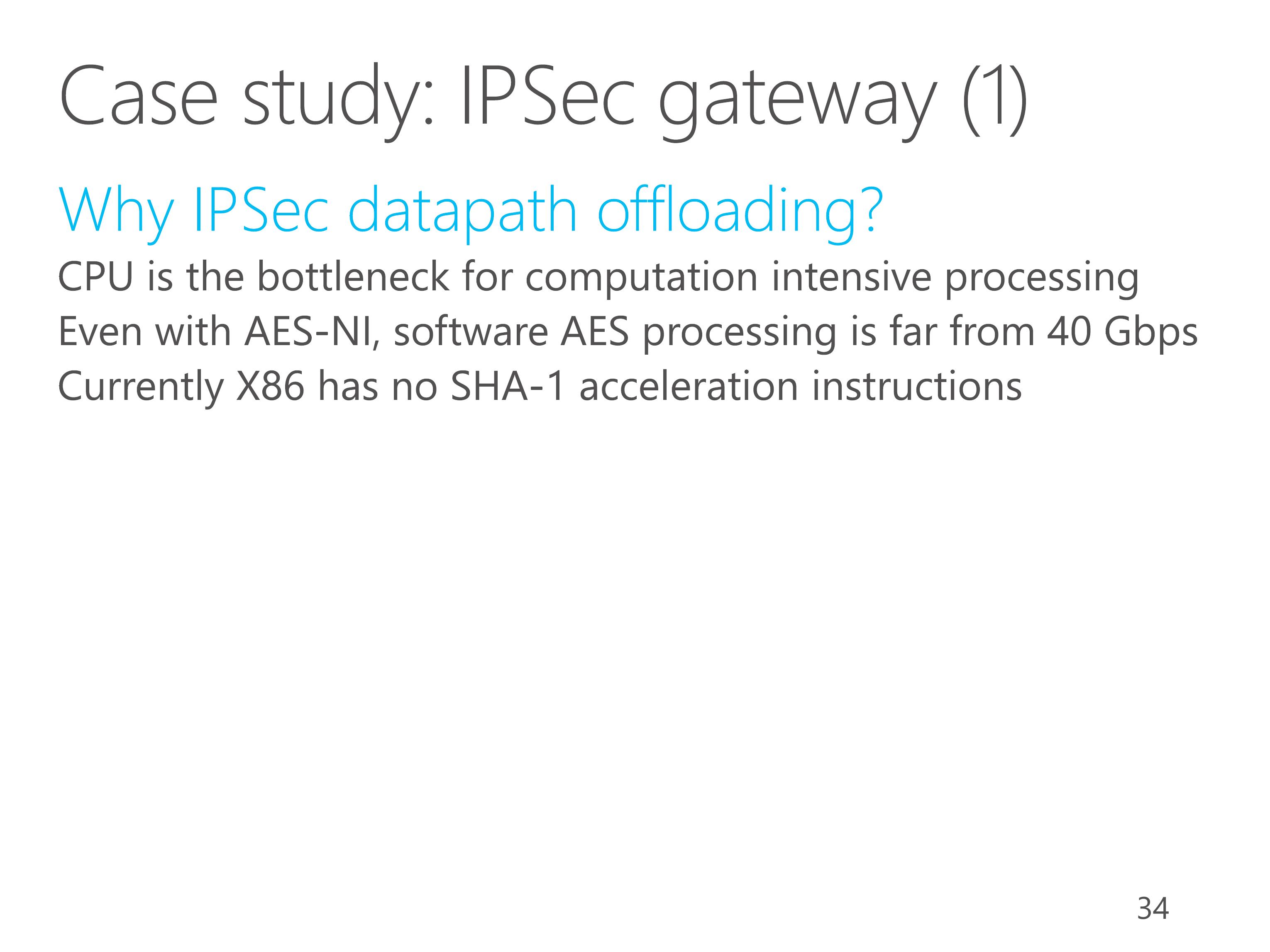
For case study, here we show an example network function, IPSec gateway.
The datapath of IPSec gateway uses AES for encryption and SHA-1 for authentication, which is computation intensive.
Although CPU has AES-NI acceleration instructions, the throughput of software AES processing is still far from 40 Gbps.
Furthermore, currently there is no instructions to accelerate SHA-1 operations.
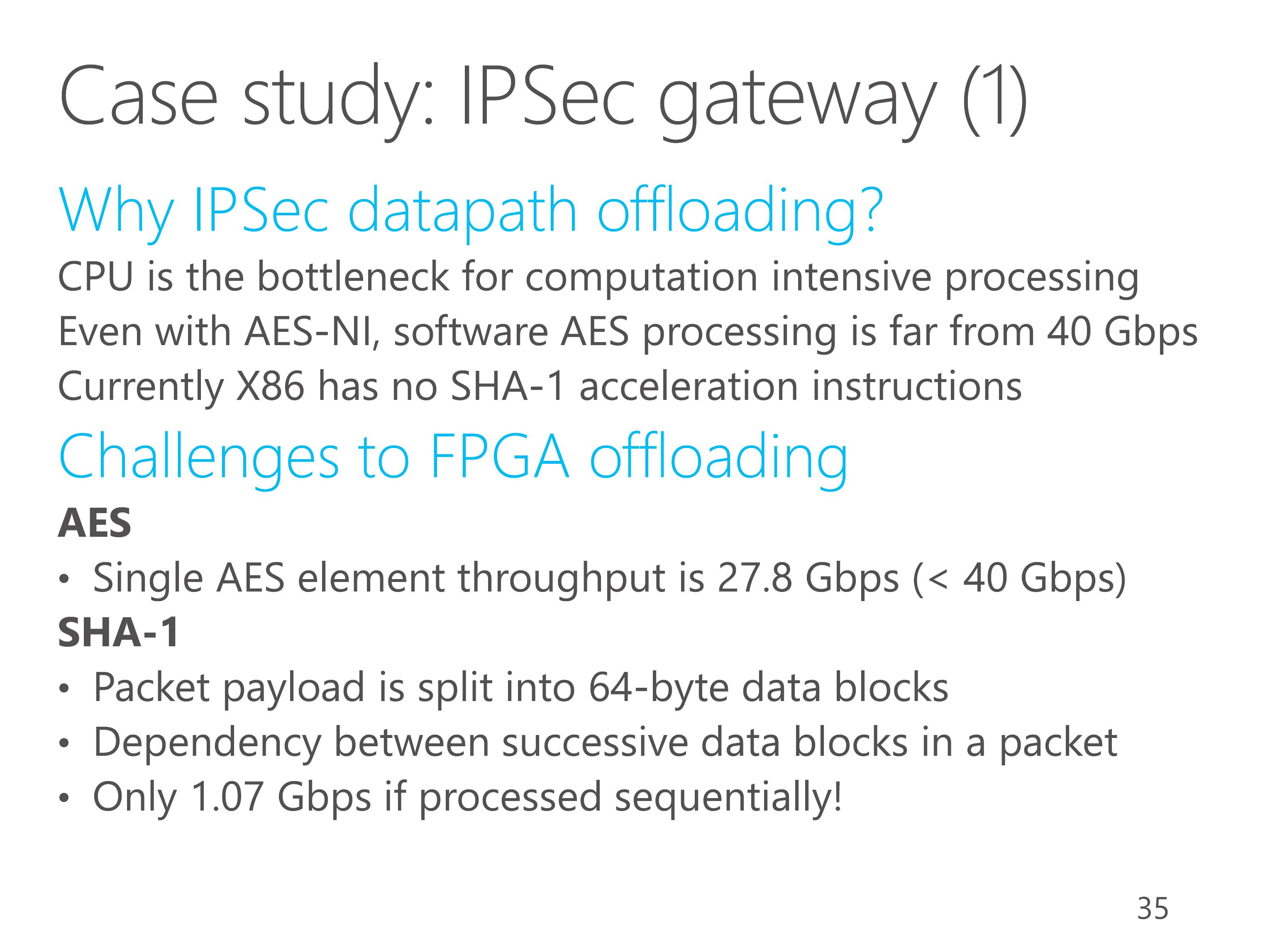
There are two challenges in offloading IPSec datapath to FPGA.
For the AES part, a single AES element does not have enough throughput.
For the SHA-1 part, each packet payload is split into 64-byte data blocks.
There is dependency between successive data blocks in a packet, which means a data block cannot start processing before the previous one is finished.
If the packets are processed sequentially, the throughput will only be 1 Gbps.
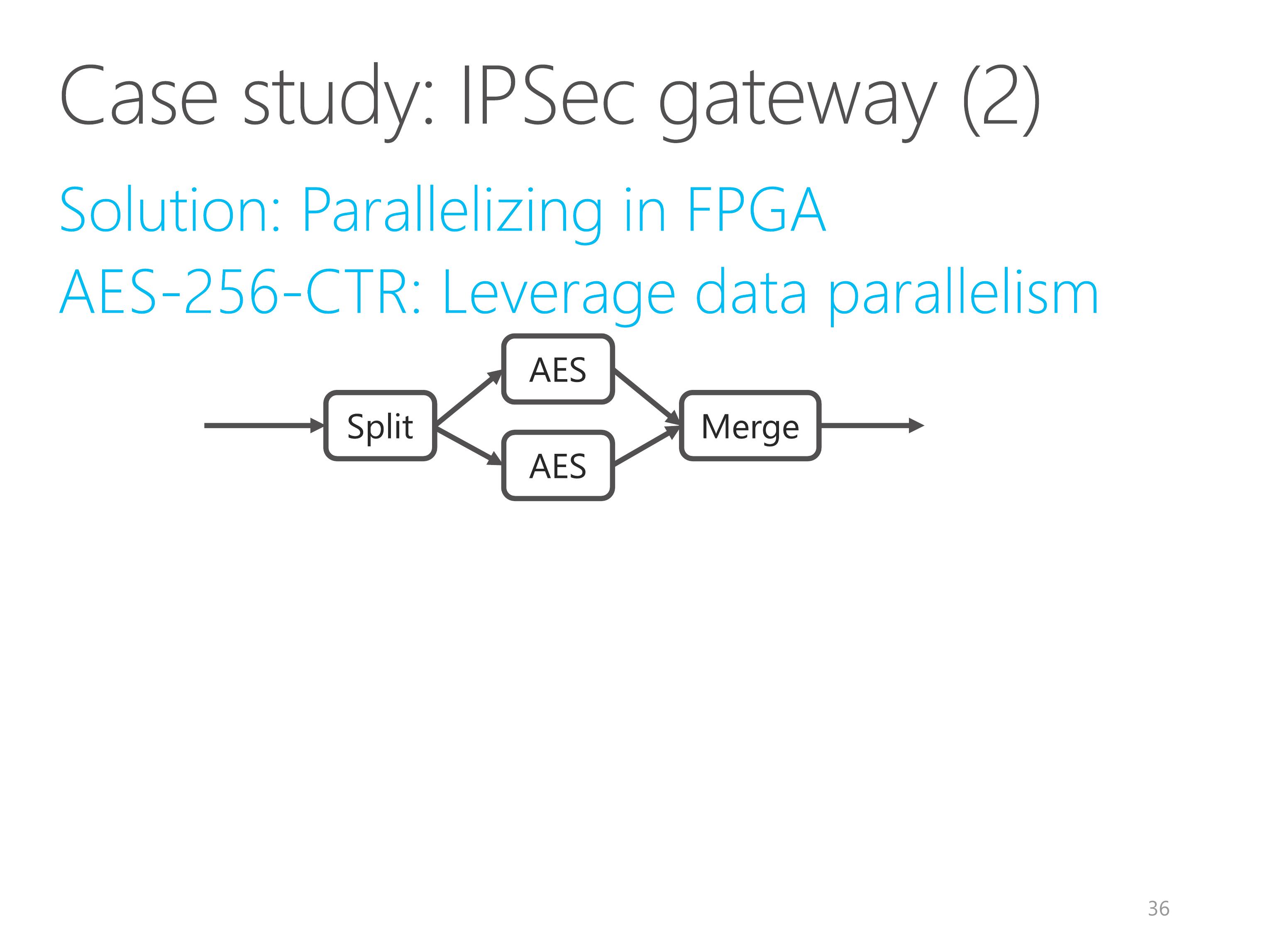
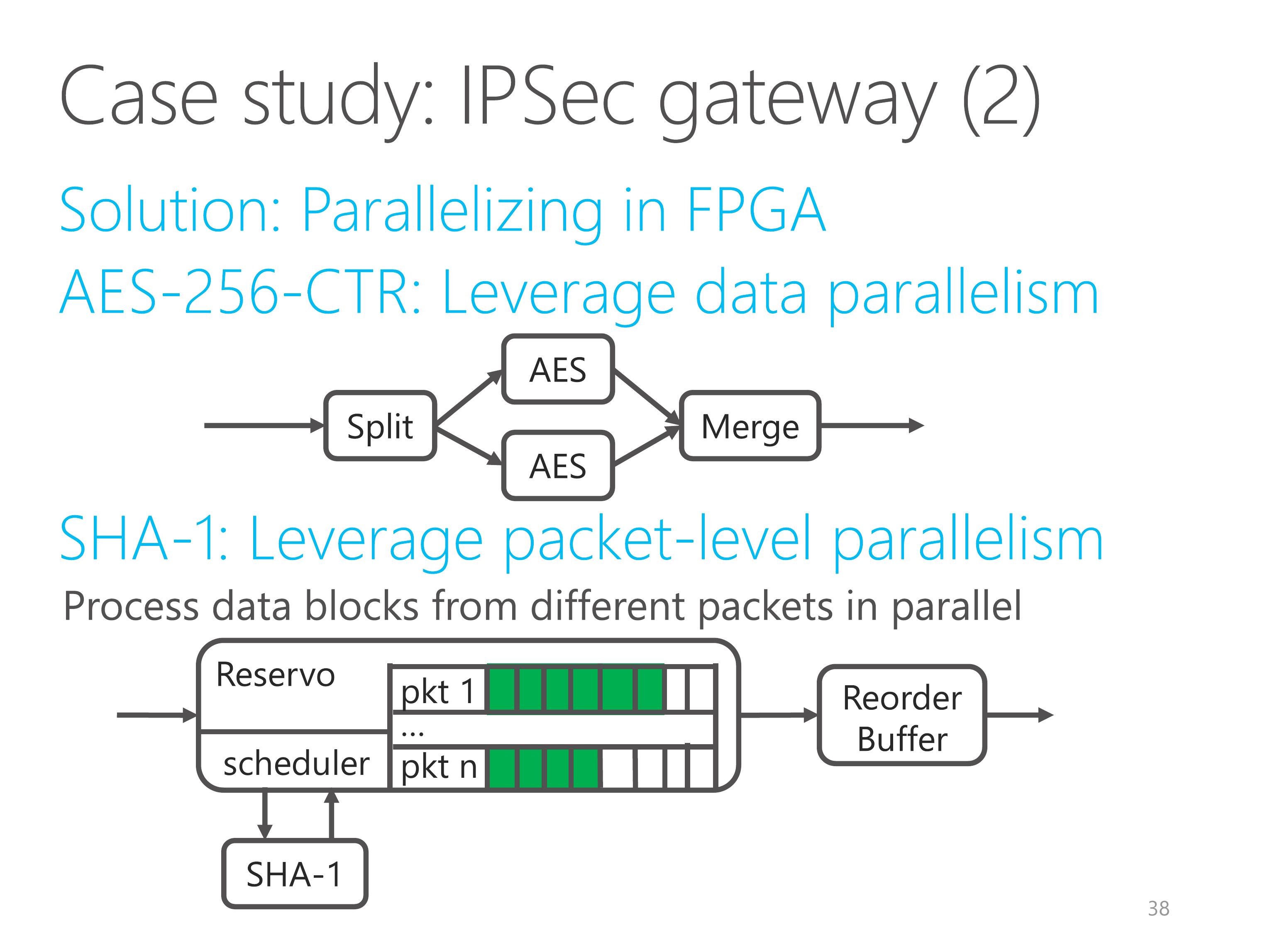
Our solution is to leverage two kinds of parallelism in FPGA.
AES encryption in counter mode can be parallelized relatively easily.
We leverage data parallelism and duplicate the AES element.

For the SHA-1 part, we leverage packet-level parallelism, because data blocks from different packets can be processed in parallel.
The reservo element buffers all the packets and schedules independent data blocks to the SHA-1 element.
Another subtle problem is packet out-of-order.
Because larger packets have more data blocks and have higher processing latency, the output packets from the Reservo element may get out of order.
So we add a reorder buffer element to recover the original packet ordering according to packet sequence number.
The reservo buffer size and reorder buffer size are less than 100 kilobytes.
Due to the flexibility of ClickNP, leveraging data and packet-level parallelism is pretty easy.
With C language and ClickNP framework, the three elements require less than five hundred lines of code and the development only takes one week.
However, if we use Verilog, it may require several thousand line of code and the development may take several weeks or even several months, if you are unlucky.
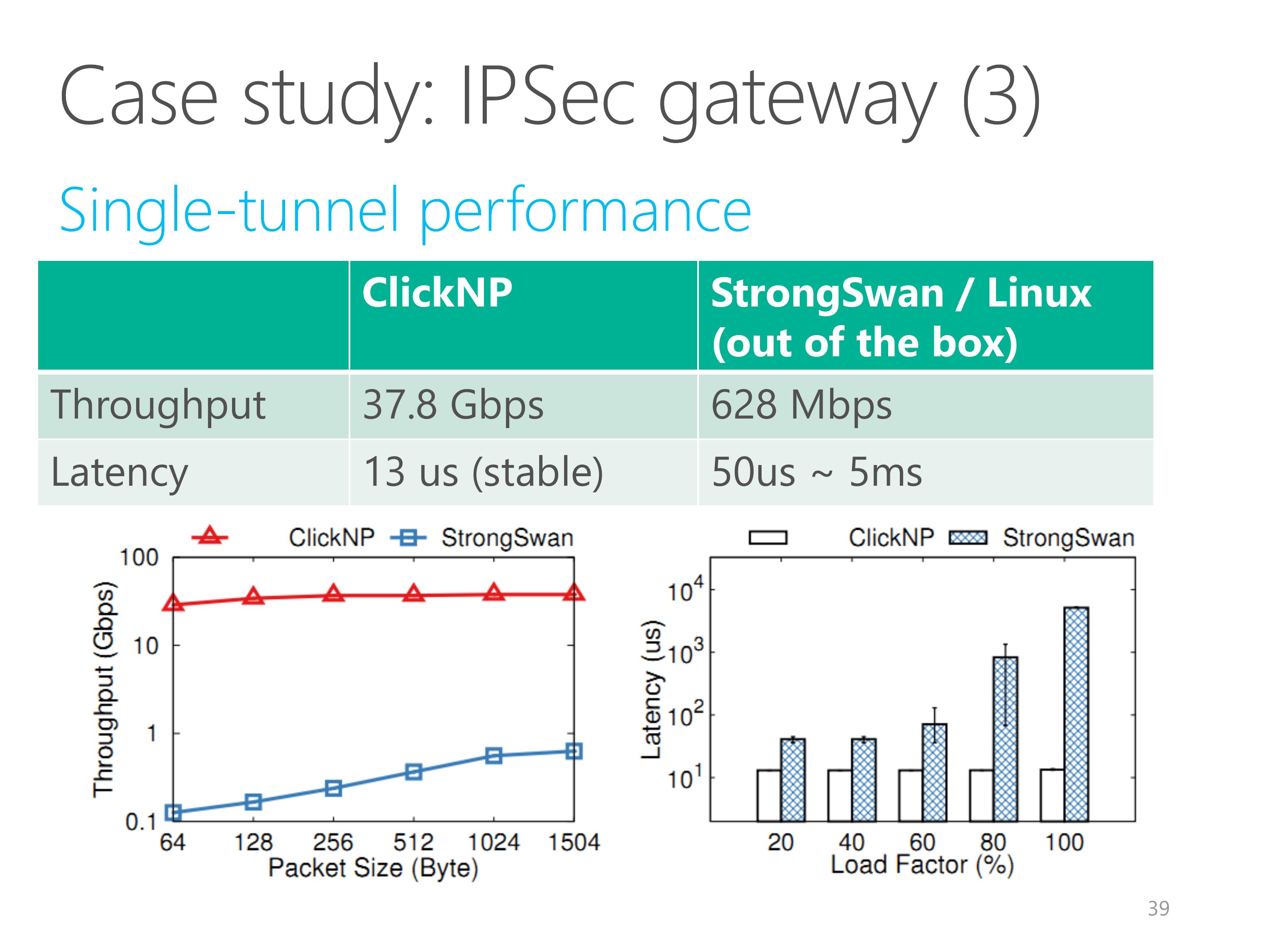
We evaluate the single-tunnel performance of ClickNP, compared to a software network function, StrongSwan on Linux.
We used StrongSwan out of the box and did not try to optimize it.
Our IPSec gateway implementation on FPGA achieves 40 Gbps line-rate for any packet size.
The latency of our IPSec gateway is also much lower and much more stable than the CPU counterpart.
When the load factor is high, The latency of Linux will grow quickly.
The second application I want to show here is a layer-4 load balancer.
L4 load balancer is a critical network function for Azure data center.
Every packet going into the data center hits the L4 load balancer.
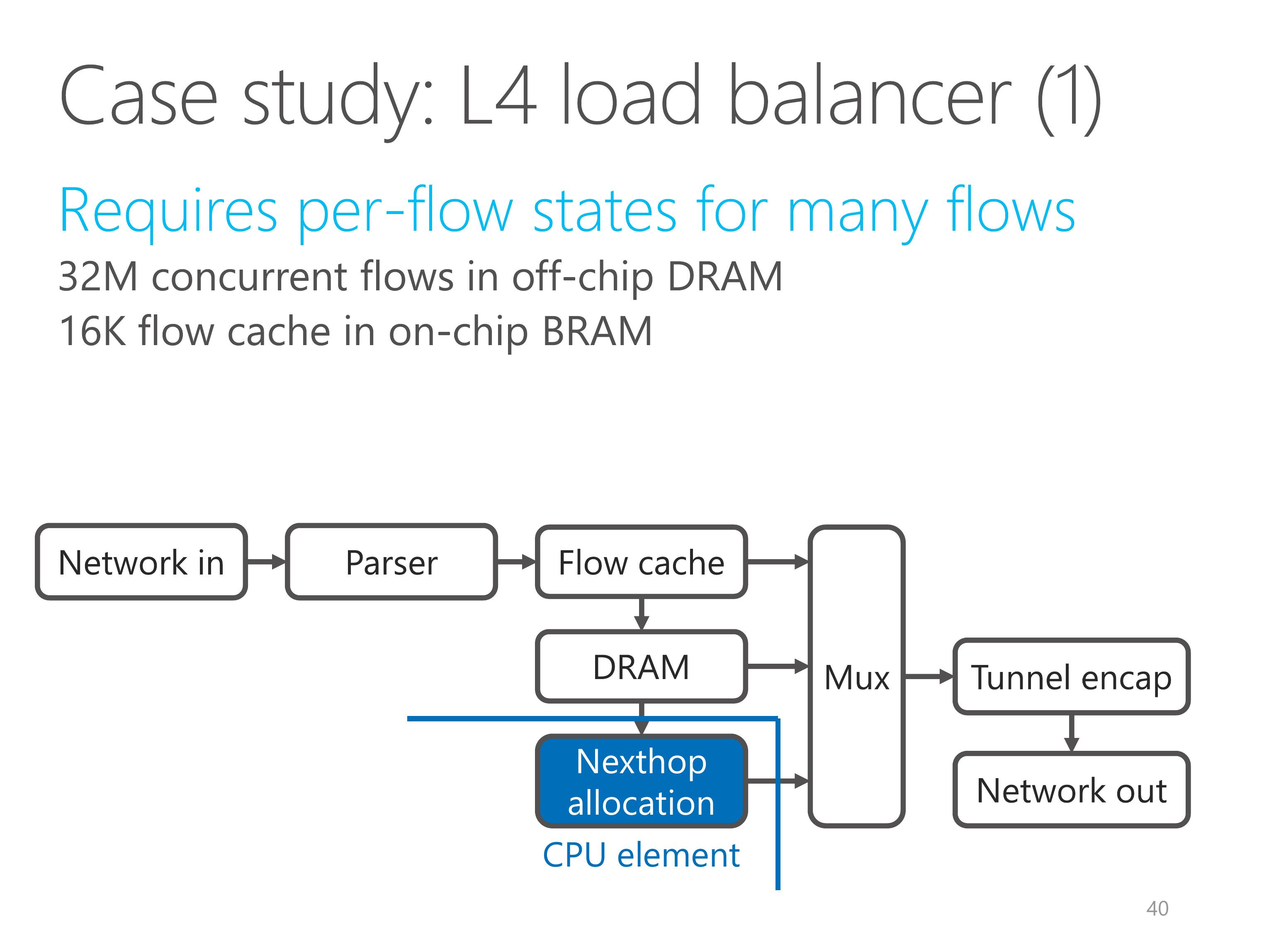
So the L4 load balancer requires per-flow states for a large number of flows.
We maintain per-flow states in off-chip DRAM for 32 million concurrent flows.
Because DRAM access is slow, we design a flow cache with 16 thousand entries.
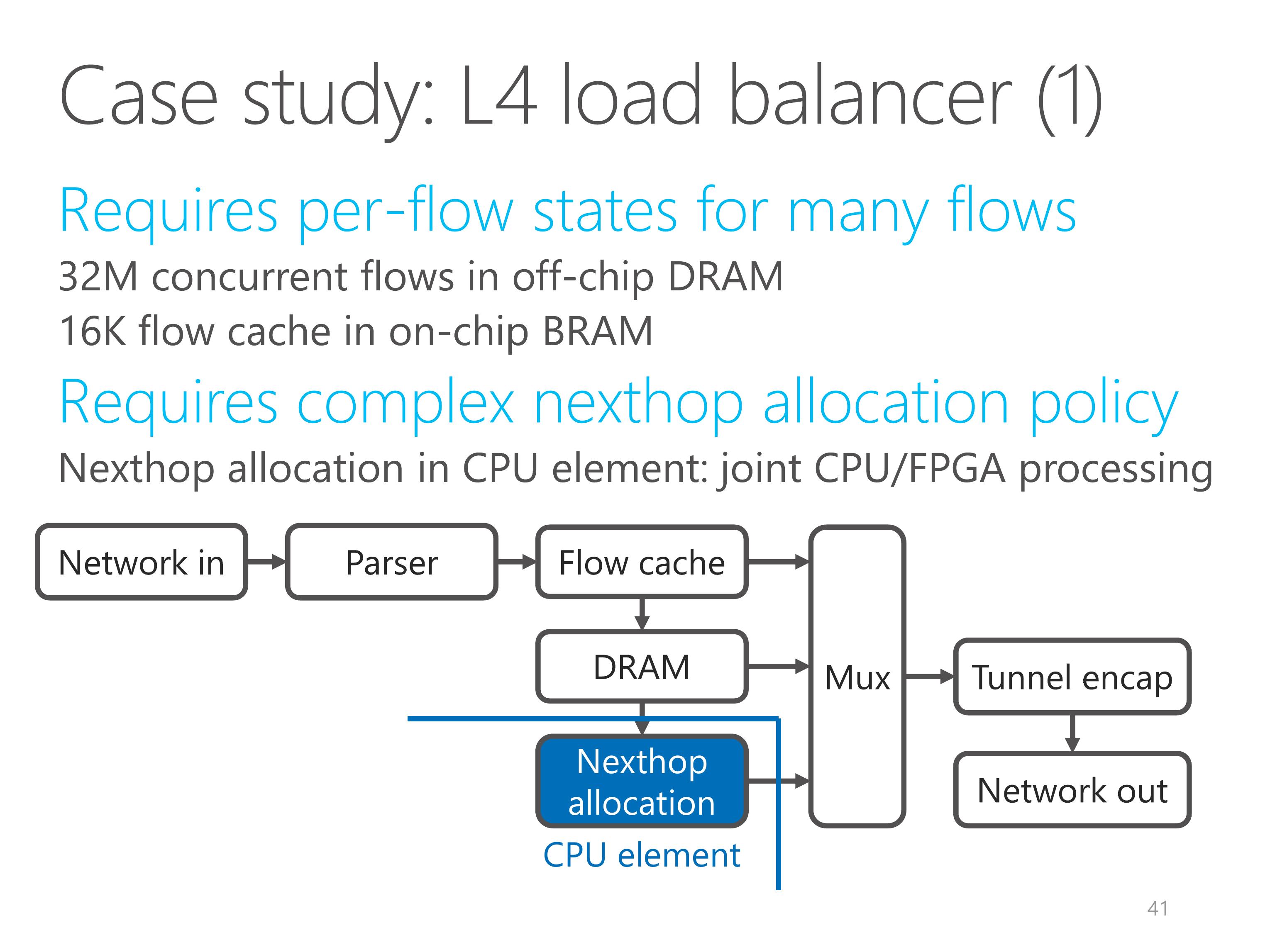
The second requirement is complex nexthop allocation policy.
This policy is more suitable to run on CPU.
So we put the nexthop allocation element on CPU, which is an example for joint CPU and FPGA processing.
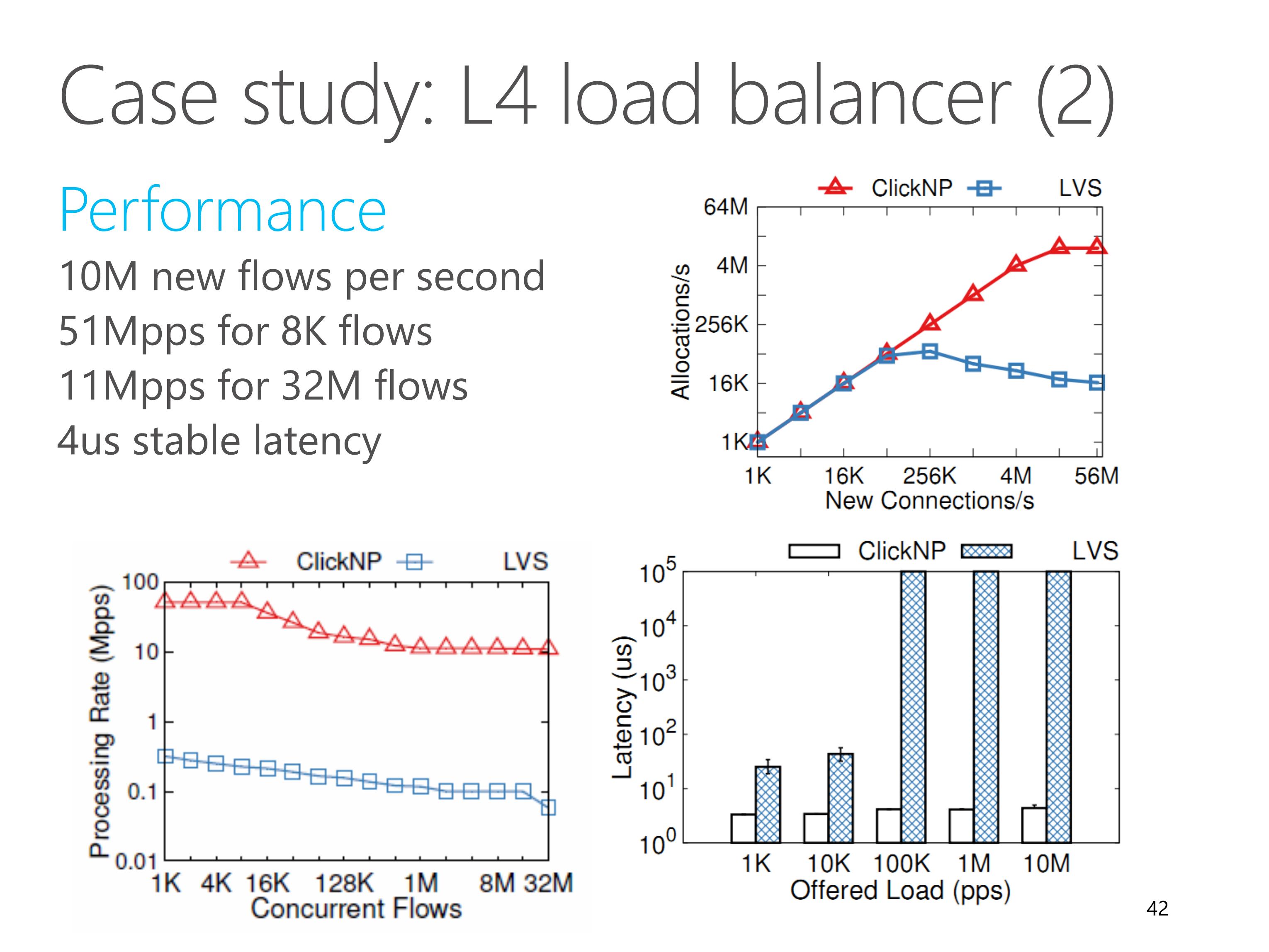
The L4 load balancer can sustain 10 million new connections per second.
The bottleneck is DRAM random access, instead of PCIe I/O channel to communicate with the nexthop allocation element on CPU.
When the number of concurrent flows is small, the throughput can achieve 50 million packets per second.
When the number of concurrent flows exceed flow cache size, the throughput begins to decrease due to cache miss.
The L4 load balancer also has microsecond-scale stable latency.
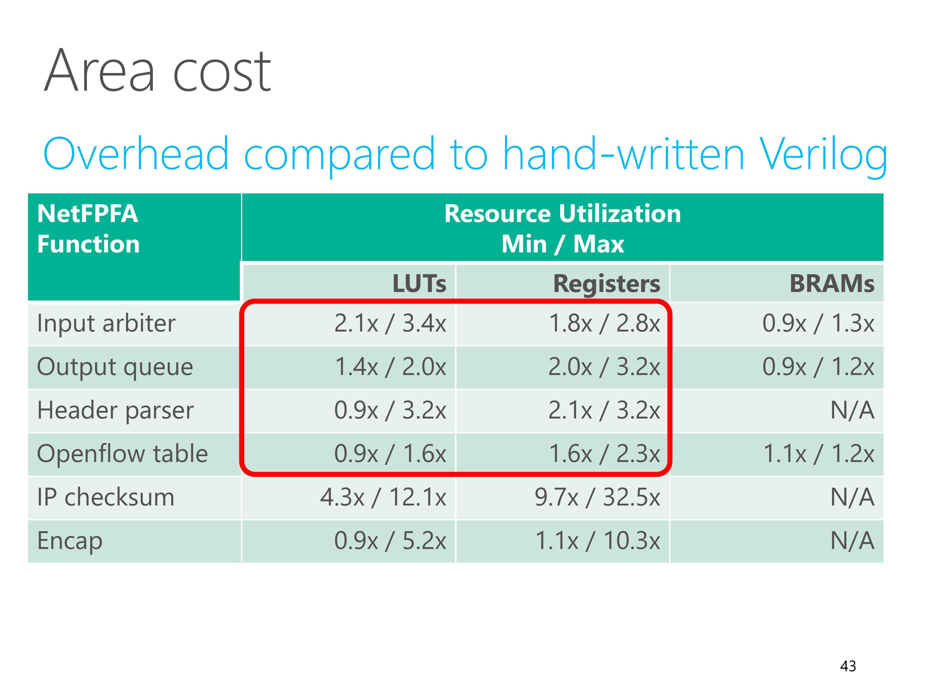
Finally, we study the area cost overhead of ClickNP compared to hand-written Verilog.
We pick up NetFPGA, which comes from Stanford and has good code quality.
For ClickNP, we implement equivalent functionality of several NetFPGA functions.
For most elements, overall the area cost overhead is less than two times.
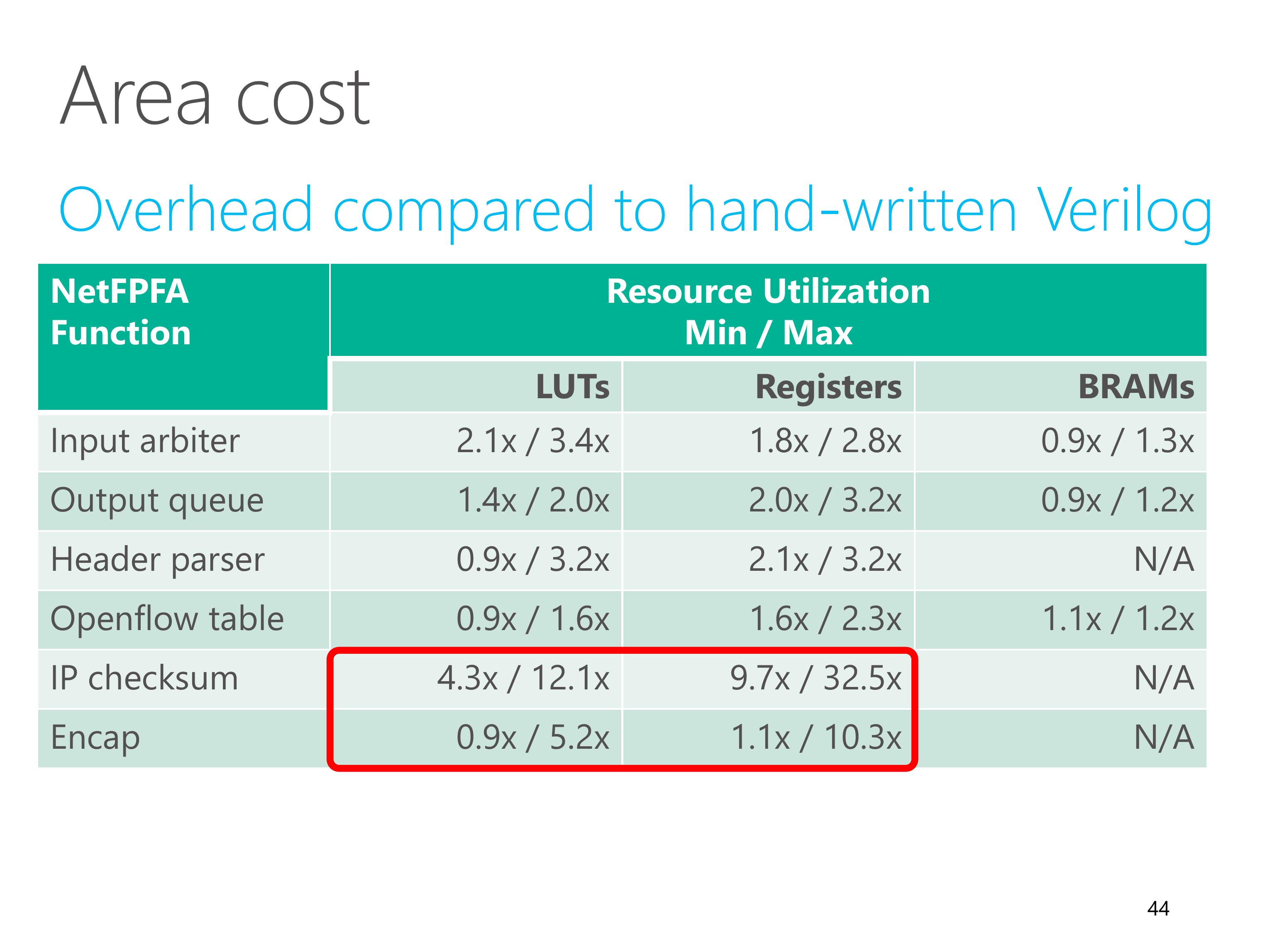
For small elements, the overhead is relatively large, but the absolute overhead is small.
This is because every element is compiled to a logic block. High-level synthesis tools generate a wrapper with a fixed logic overhead.
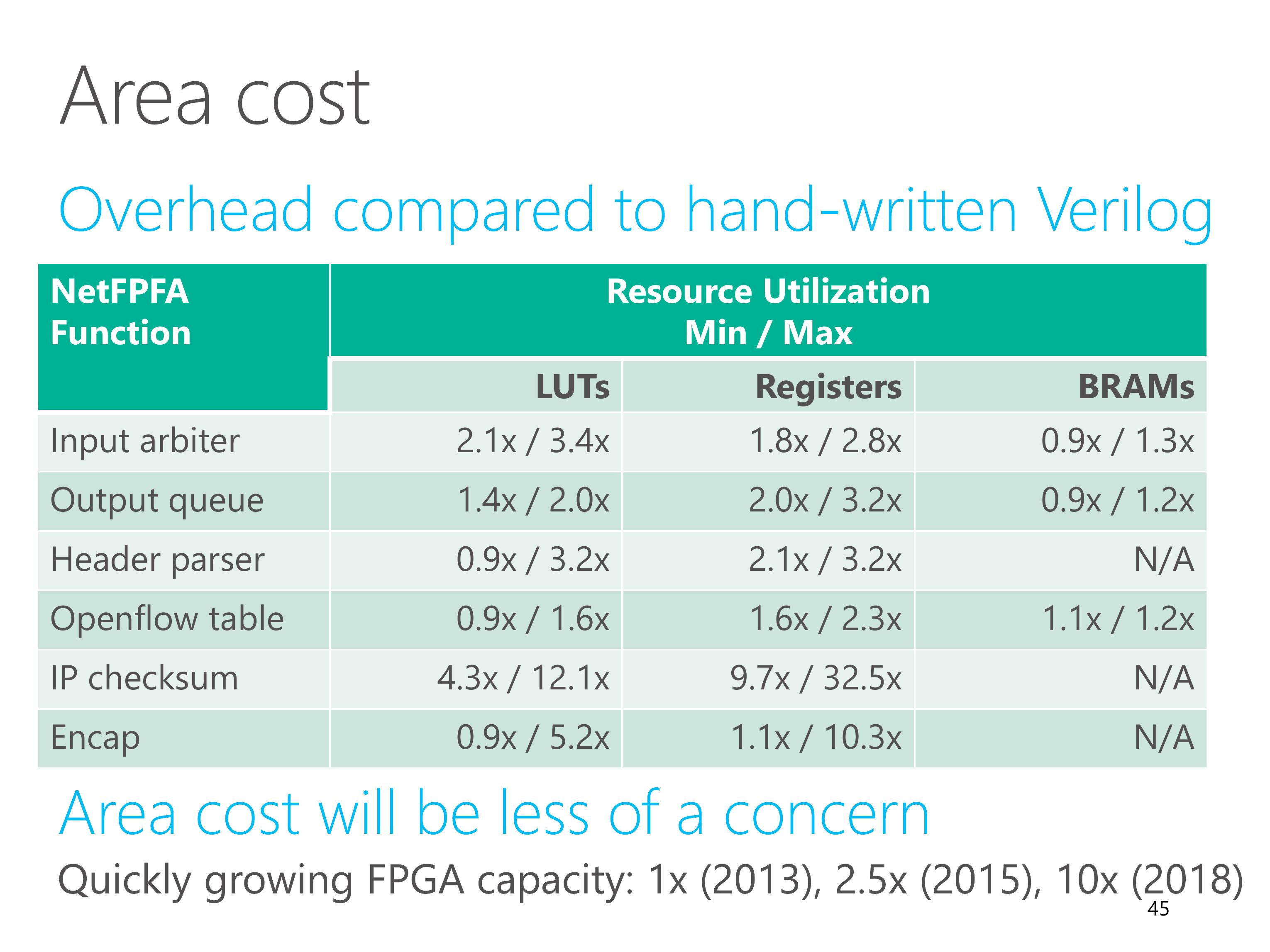
Furthermore, the capacity of FPGA is growing quickly in recent years.
We believe that the area cost will be less of a concern in the future.
Finally, the conclusion.
FPGA is fast, general and mature, so we have deployed FPGA at scale in the cloud.
This work presents ClickNP, a network processing platform to enable software developers to program hardware, which is highly flexible, modular, high performance and supports joint CPU/FPGA packet processing.
In addition to network processing, ClickNP is a general framework for programming on FPGA.
With FPGAs in datacenters, we can go beyond the memory wall and reach a fully programmable world.

Please check out our demo on Thursday.
Thank you for listening!